Making my own 100 W USB-PD programmable power supply
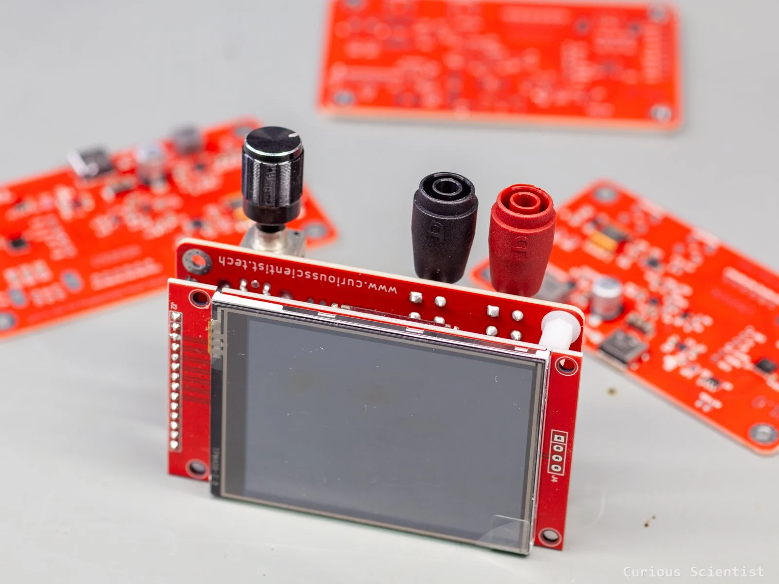
In this article, I show you how I designed my own USB-PD (power delivery) programmable power supply (PPS). USB-PD is becoming more and more popular nowadays. I already touched upon the topic when I developed my, first of its kind, USB-PD-compatible breadboard power supply. The power supply can be used to negotiate the typical PD voltage levels between 5-20 V, while the board also provides the typical rail voltages, 3.3 V or 5 V, whichever was selected by the user. This time, I tried to take a bit bigger step: I developed a circuit and firmware based on the CH32X035G8U6 microcontroller. Actually, it is not “just” a circuit and its firmware, but a full product. I added a 2.8” LCD, an INA226 high-resolution power meter, an LM73100 ideal diode, proper banana plugs, and I designed a nice 3D-printable enclosure for the whole thing. So, it is a complete programmable power supply.
Introduction
The board is based on the CH32X035G8U6 microcontroller. I picked this microcontroller because its development board is easily available from AliExpress, and it supports everything I need. It has native USB and PD PHY, so it can deal with power delivery, and it has all the typical peripherals that one might need: ADC, SPI, UART, I2C, etc. It has a built-in 48 MHz oscillator, so the circuit does not require an external one. Its operating voltage range allows both 3.3 V and 5 V operation. It has 20 KB RAM and 62 KB flash, which is a great leap from the V003 series’ 2 KB RAM and 16 KB flash, but it even out-competes the V006 series’ 8 KB RAM (however, same flash). This specific chip (G8U6) comes in a QFN28 package. It is fairly small, but allows a lot of GPIOs. As usual, I developed the firmware in MounRiver Studio II.
The firmware features the following:
Full-featured communication with USB-PD power adapters.
Status reporting through USART
Power status and power enable/disable via the LM73100 ideal diode
Displaying status and telemetry on a 2.8” ILI9341 LCD
Navigating via a rotary encoder
Measuring output power (current, voltage, power, energy, etc.) using an INA226 chip
The circuit has a lot of principles merged, and initially, I found the project quite intimidating because there were some components or sub-circuits that I had no prior experience with. But I trusted the good old RTFM* approach, and it seems that it worked! I spent weeks reading the datasheets of the different chips and understanding their reference designs, and then implementing them into my circuit.
The circuit features the following:
CH32X035G8U6 microcontroller for USB-PD communication, display control, ideal diode control and power meter control
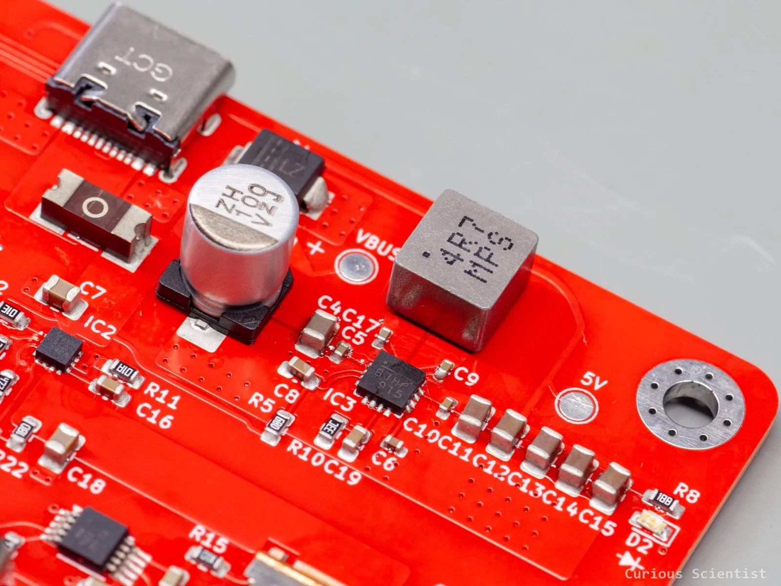
MP28167 Buck-boost converter that accepts voltages between 3.3 V and 20 V and outputs a stable 5 V
TLV76733DRVR low dropout regulator that feeds the whole board’s 3.3 V rail
LM73100 ideal diode that switches output power ON/OFF and provides a certain level of protection
INA226 power meter chip that allows a high-resolution output power (current and voltage) measurement
…and other small circuits and components that allow the whole circuit to operate properly
*RTFM: Read The Fucking Manual.
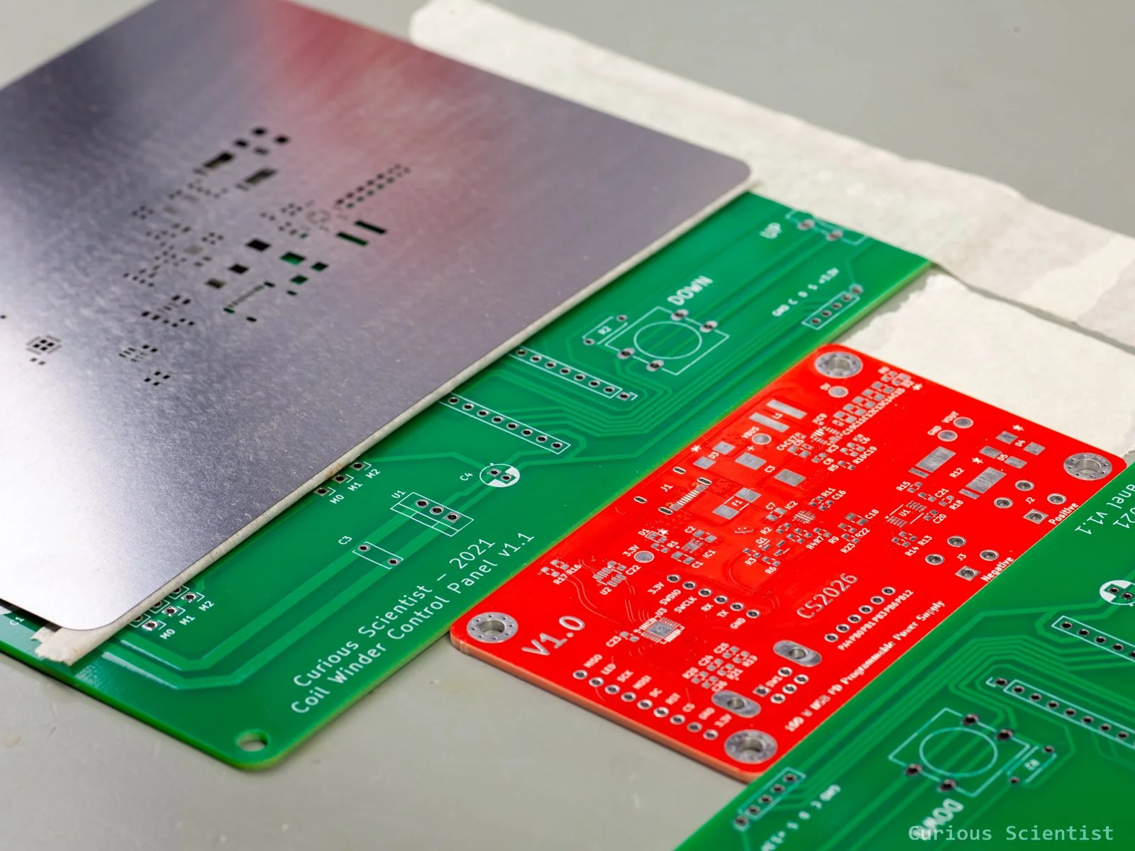
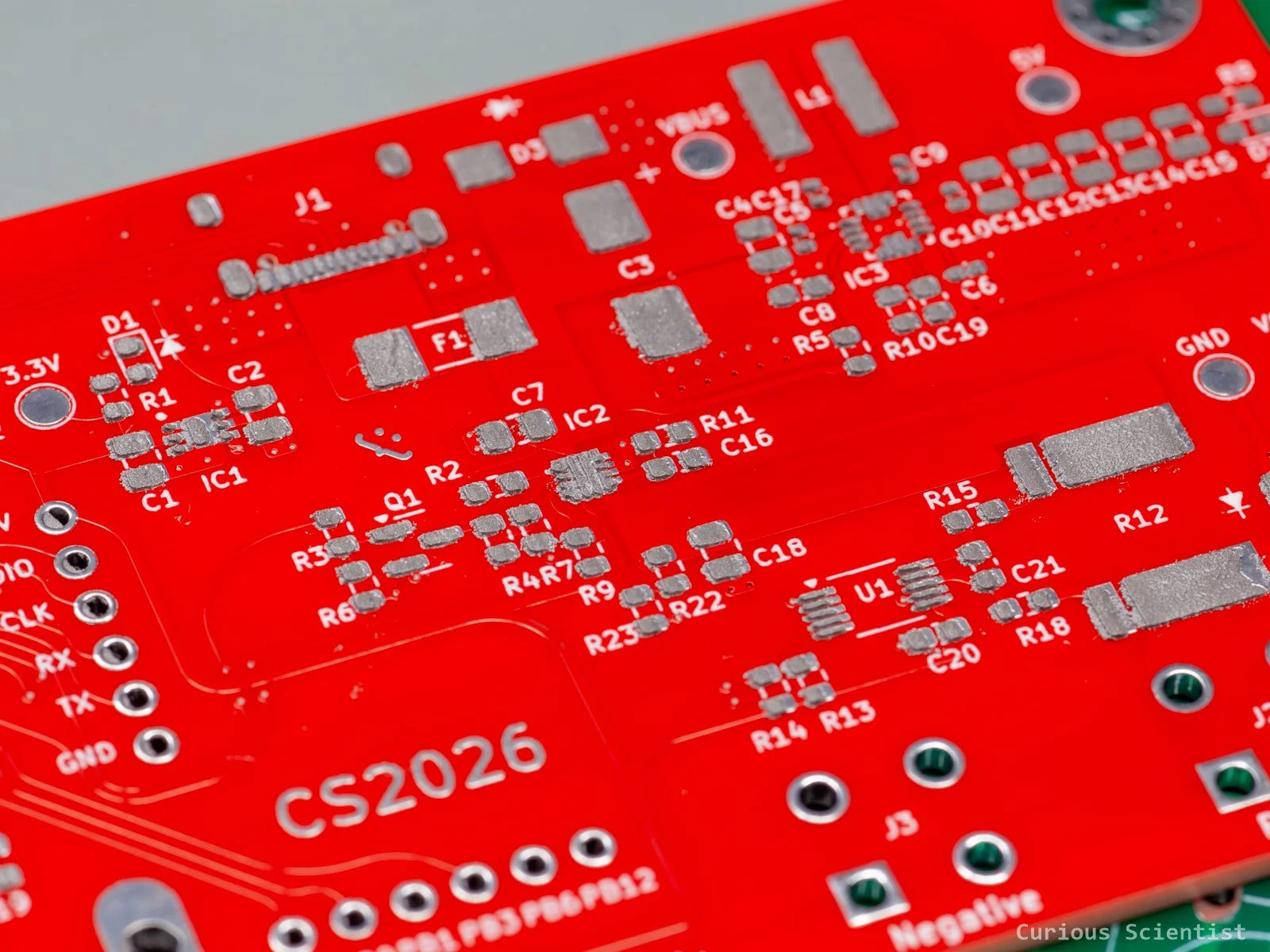
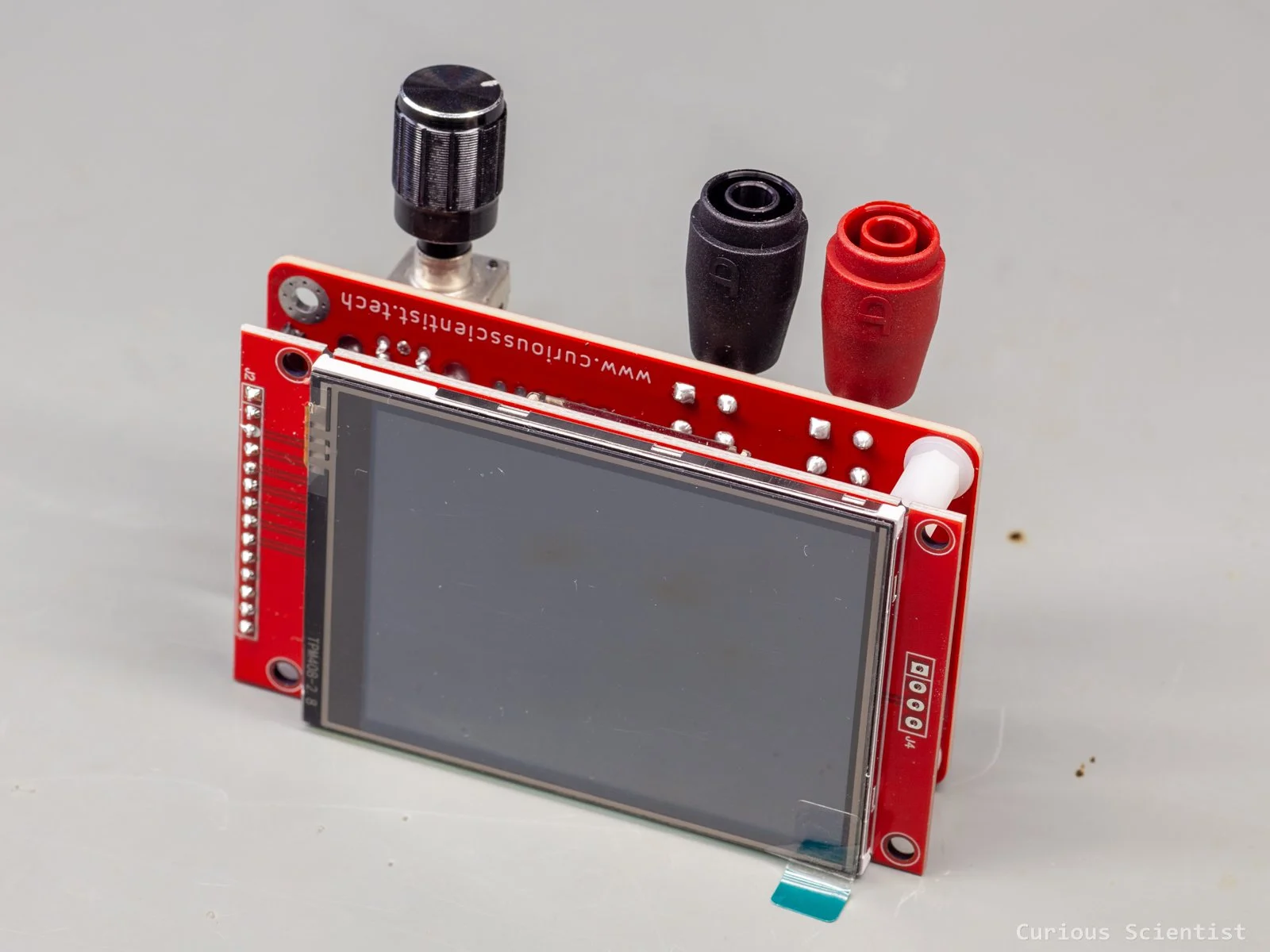
Raw PCB, this time, in a strong red color
CH32X035G8U6 microcontroller
MP28167 Buck-boost converter
I would start by discussing the “most difficult” part of the circuit.
So, the concept of the whole circuit is to be able to negotiate the typical USB PD/PPS voltages and make them available on its output. This negotiated voltage can be anything between 3.3 V and 20 V. While the PDO (power data object) voltage levels are 5 V, 9 V, 12 V, 15 V and 20 V, the PPS (programmable power supply) voltages can be between 3.3 V and 21 V, depending on the power adapter’s capabilities. Therefore, I had to prepare the circuit to operate at both low voltages, such as 3.3 V and higher voltages, such as 21 V. A simple LDO would work at low voltages, but at 21 V, even though there are LDOs that can drop down to 3.3 V, it would be a huge waste of power and a lot of heat generated.
So, my attention was directed towards switching regulators. I initially wanted to use a simple buck converter, but I could not find one that could work between 3.3 V and 21 V. Then I thought, let’s look at buck-boost converters and let’s aim for something that can accept the previously mentioned range and can provide a stable 5 V output voltage.
The MP28167 works between 2.8 V and 22 V and can provide up to 3 A of current while delivering a fixed 5 V output voltage. BINGO!
I looked up its datasheet and read it carefully, especially the PCB layout guidelines chapter. I also discovered that the chip has an evaluation board whose datasheet provides further layout guidance and even a suggested BOM. The evaluation board’s guidelines, however, scared me a bit because it was suggesting a 4-layer board and I wanted to avoid that. So, I took the risk and implemented the layout on a 2-layer board. It worked!
Buck-boost converter, based on the MP28167 chip
TLV76733DRVR Voltage regulator
So now, as we have a stable 5 V output from the buck-boost converter, we need to get this voltage converted to 3.3 V. Although all the components could work at 5 V, some versions of the display do not like 5 V, so I decided to make the whole circuit operate at 3.3 V. It is safer.
I picked this LDO because it is relatively modern. Still nowadays, people go for the good old LM1117 voltage regulator, because it just works. There are lengthy discussions on Reddit about why the LM1117 and its analogues must be avoided. One thing is that it burns 5-10 mA just by sitting in the active circuit (quiescent current). The TLV767 only uses 50 uA, which is 1-200x smaller!
The chip does not require any difficult layout design, and as usual, an accurate layout guideline can be found in its datasheet. Since the chip only needs two capacitors, it is really not rocket science, especially after laying out the buck-boost converter circuit.
3.3 V voltage regulator circuit based on the TLV76733DRVR voltage regulator
LM73100 Integrated ideal diode
This component is a fun one! It is a circuit protection device that can protect against voltage surges, reverse polarity and so on. It is an ideal, must-have choice for power supply circuits. It not only provides protection, but it can also be used as a power switch. Ideal for my circuit where I want to enable/disable the output.
Its operating range is between 2.7 V and 23 V, and it can conduct up to 5.5 A continuously. It is a diode because it only lets the current flow in one direction, and it is ideal because it does this while not punishing the circuit with a forward voltage drop (and therefore heat!) of ~1 V. This is thanks to its inner workings based on two back-to-back FETs whose total typical resistance is only around 30 mOhm. This results in a basically negligible voltage drop and heat generation.
The chip’s circuit contains several considerations. First, the chip can be enabled/disabled from the microcontroller. This is done by switching a BSS138 MOSFET with one of the MCU’s GPIO pins. The MCU also reads the PG (power good) pin of the chip. This is an open-drain pin, and it is pulled up to 3.3 V using a 4.7 kOhm resistor. When the power path is fully turned on and the PGTH (Power good threshold) input exceeds a certain threshold, the signal goes high on this pin. When the voltage on the PGTH pin goes above 3 V, the PG pin goes high. The voltage is carefully set using a voltage divider fed from the switched power rail.
Apart from the power good status, there are two other important features that are used. They are related to the EN/UVLO (enable/undervoltage lockout threshold) and OVLO (overvoltage lockout threshold) pins. Both pins share the output junctions of a three-resistor-voltage divider. According to the device’s datasheet, they work in the following way. Based on the formula provided in the datasheet, we can calculate a cutoff voltage level below which the device applies undervoltage protection. Along the same principles, there is an overvoltage protection as well. There is a similar formula that is based on the same voltage divider’s other junction. If the input voltage crosses the OVLO threshold, the device turns the power off. In both UVLO’s and OVLO’s cases, we must pick the resistors in a way that the voltage divider produces 1.2 V or above at the given threshold levels. I picked the resistors so that my ideal diode is operational between 3 V (3.01 V) and 23 V (23.04 V).
Ideal diode circuit based on the LM73100 chip
INA226 - 16-bit Power Monitor
This device monitors the voltage and current after the ideal diode that goes to the positive output terminal. The device requires a shunt resistor to measure the current. I used a 5 milliOhm current sense resistor for this purpose. The resistor has four terminals, so it is ideal for Kelvin-sensing. The wide “main” tabs conduct the majority of the current, while the narrower tabs are used for sensing the voltage drop across the shunt resistor by the INA226 chip. The resistor has 3 W power rating, but even when the maximum amount of 5 A is passing through it, the dissipated power is only 125 mW and the voltage drop is only 25 mV.
While the current sensing is done between the output of the ideal diode and the positive banana terminal, the voltage sensing is done between the “output side” of the shunt resistor and the positive banana terminal. I chose this way because then the voltage drop caused by the shunt resistor is also considered and the measured voltage is the voltage that appears on the output terminal. It is not a big difference, but this way, it is a bit more correct.
The voltage drop across the shunt resistor is not directly measured by the INA226 chip. I added an RC filter between the terminals.
The INA226 chip and its 5 mOhm shunt resistor with a filter network
Further considerations and components
Apart from the main chips and sub-circuits, there are other, smaller components that play a crucial role.
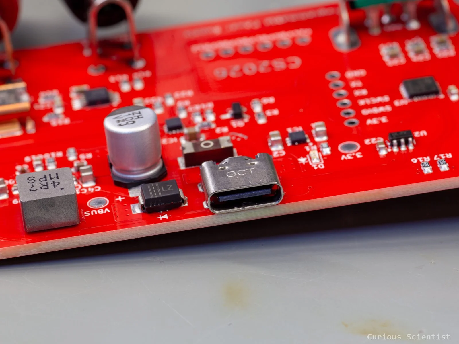
First of all, the power arrives on the board via a USB-C connector. This is nothing fancy, just a regular USB-C 2.0 connector. The VBUS line is immediately driven through a fast-acting fuse to protect everything downstream if something goes wrong and the device tries to draw too high a current. The VBUS line is also protected by a TVS diode, right at the USB port, and a bit further away, between the USB connector and the microcontroller, there is an ESD protection chip. The output terminal is also protected against ESD and transients using two separate diodes.
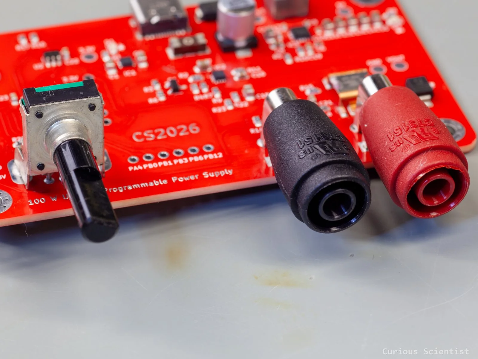
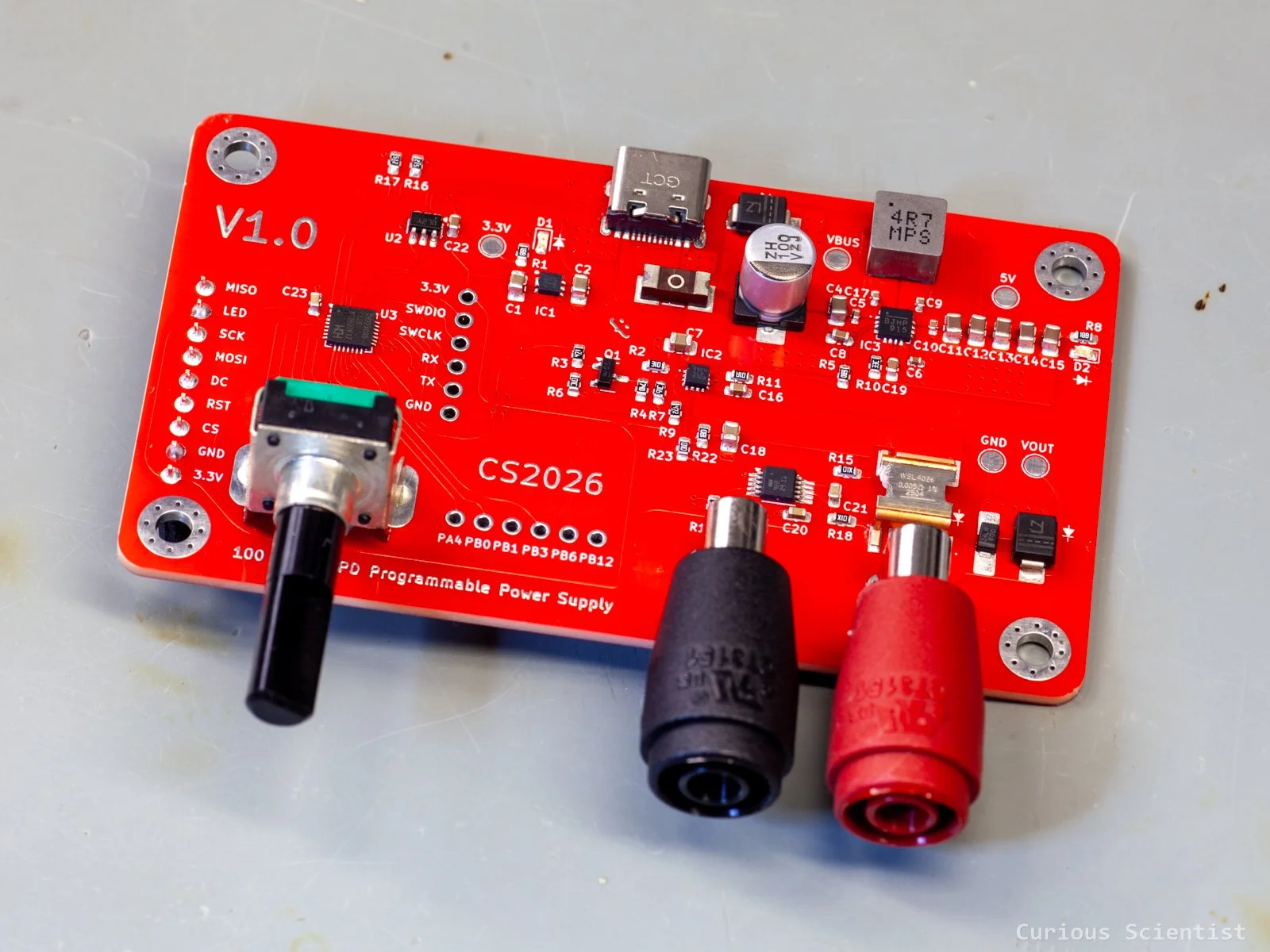
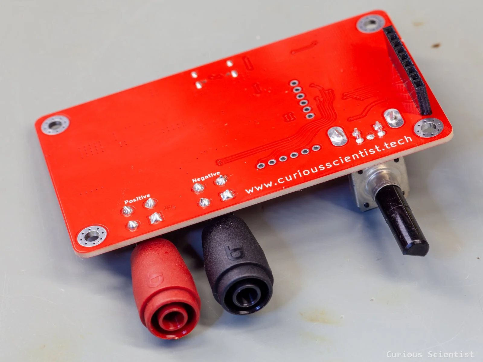
The device is controlled by a rotary encoder. I used a right-angle rotary encoder with a built-in switch. This way, I can have the encoder soldered in the PCB while it is facing the same direction as the output terminals. The output terminals are probably a bit overkill, but I wanted to make sure that they can take some abuse. So, I picked a sturdy safety jack for 4 mm plugs. They are also directly soldered onto the PCB. They connect to the PCB through four legs, which provide both a solid support and a low-resistance path.
The PCB is specifically designed to accommodate a generic 2.8” TFT LCD. The size of my PCB almost matches the display, and the pins next to the rotary encoder are specifically laid out to accommodate the display. However, since they are mainly power and SPI pins, any SPI display can be used with the board, but it might not match the pins on the PCB. But there’s always a way to solder the wires of the display. Actually, I am working on an alternative implementation that uses a large OLED display, so soon I will be able to show how to use the board with other displays as well.
Apart from the display-related pins, there are two more rows of pins on the board. One is for programming and communication. I grouped together the power pins (3.3 V and GND), the programming pins (SWDIO and SWCLK), and the serial pins (TX and RX). It is important to notice here that, unlike the V003-series, this chip needs both programming pins to be connected to the programmer during programming! The third pin group is just the leftover pins from the MCU. I made them available, so those who want to expand my board and want to use more GPIOS can access six additional pins.
As usual, the board has rounded corners and four M3 mounting holes with metal plating. This way, it should be easy to mount the board in an enclosure.
Since the circuit can have three different voltage levels, I added multiple test points to it. One can check the 5 V output of the buck-boost converter and the 3.3 V output of the LDO voltage regulator to make sure that all the onboard circuits are powered properly. Furthermore, there is a VBUS test point that should reflect the negotiated voltage, and there is a VOUT test point, which is the voltage on the output.
Assembly and enclosure
The device is designed so that it can be mounted in an enclosure.
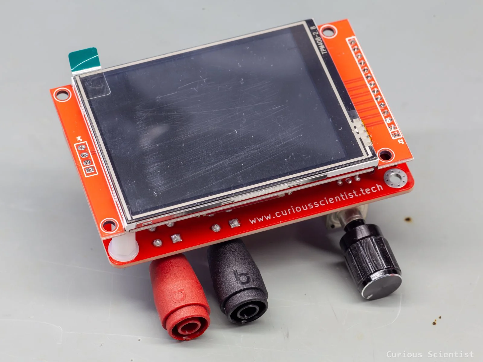
As I mentioned above, the circuit board is designed so that it can accommodate a generic 2.8” display. This display is connected to the PCB via the 2.54 mm socket on the back side of the board.
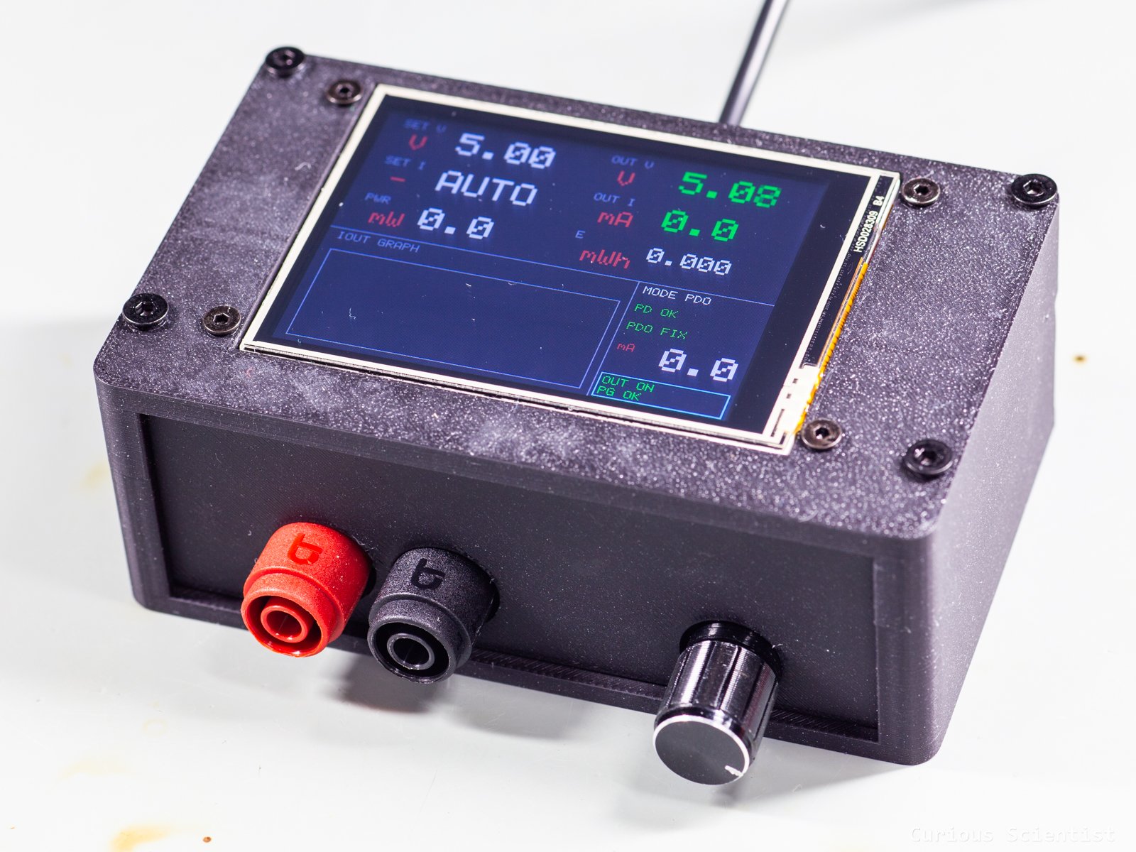
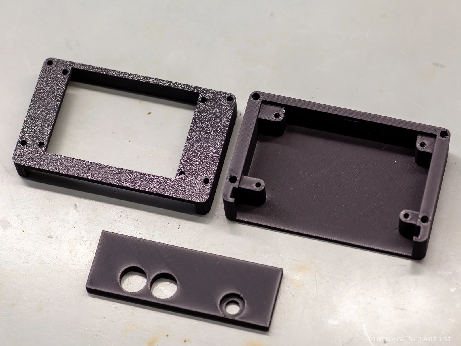
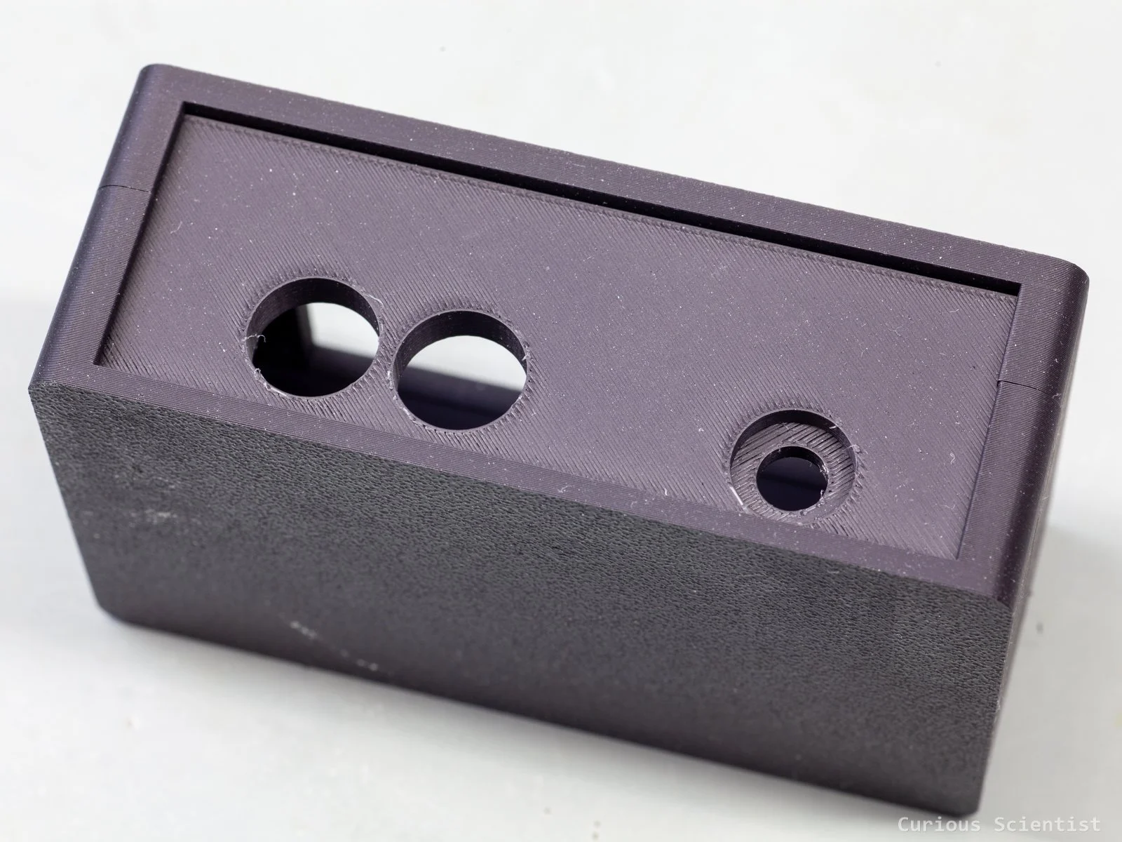
I designed a simple enclosure for the whole device. It is made of three parts: a front panel, a top shell and a bottom shell.
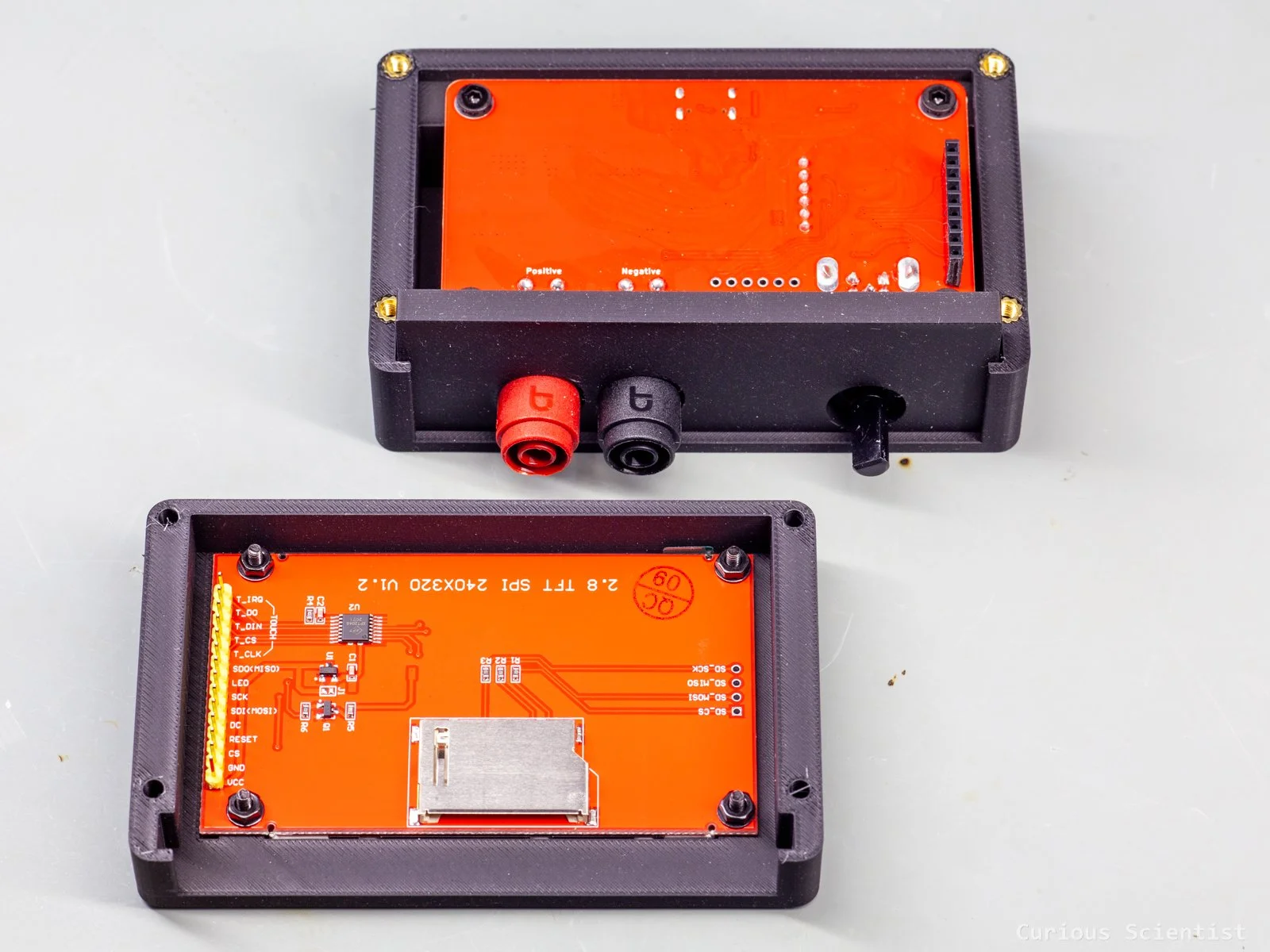
First, the front panel is mounted on the connectors. Then, the main PCB, without the display, is mounted on the bottom shell. The board sits on four supports. I could not print wide enough supports to comfortably accommodate a brass insert nut, so I just made it with slightly undersized holes, and I screwed the bolts directly into the plastic. They do not need to have any mechanical strength, so it is good enough. On the other hand, the bottom shell received four brass insert nuts for attaching the top shell to it. I had enough space and material for them, and it is more necessary here because I might disassemble the enclosure multiple times.
Once the board is in the bottom shell, the display is fixed in the top shell. This is done with four bolts and nuts using the mounting holes of the display. As a little detail, I added a tiny groove to the top shell so that the soldered terminals can sit in it so that the whole display can sit flush with the 3D-printed case. Then, the top shell with the display is carefully inserted into the terminal on the main PCB. The tolerances and distances are determined carefully, so everything sits tight.
Finally, I screwed the two shells together using four 20 mm long M3 bolts.
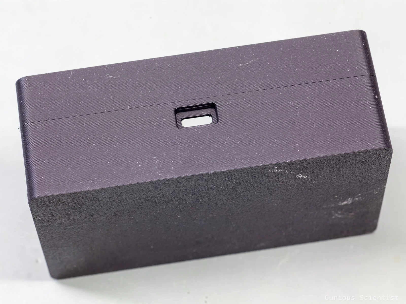
On the back side of the bottom shell, around the USB-C connector, I designed carefully, so one can use different USB-C connectors. Some USB-C connectors are shorter, or their plastic casing is thicker, so I had to take that into consideration.
Software and UI
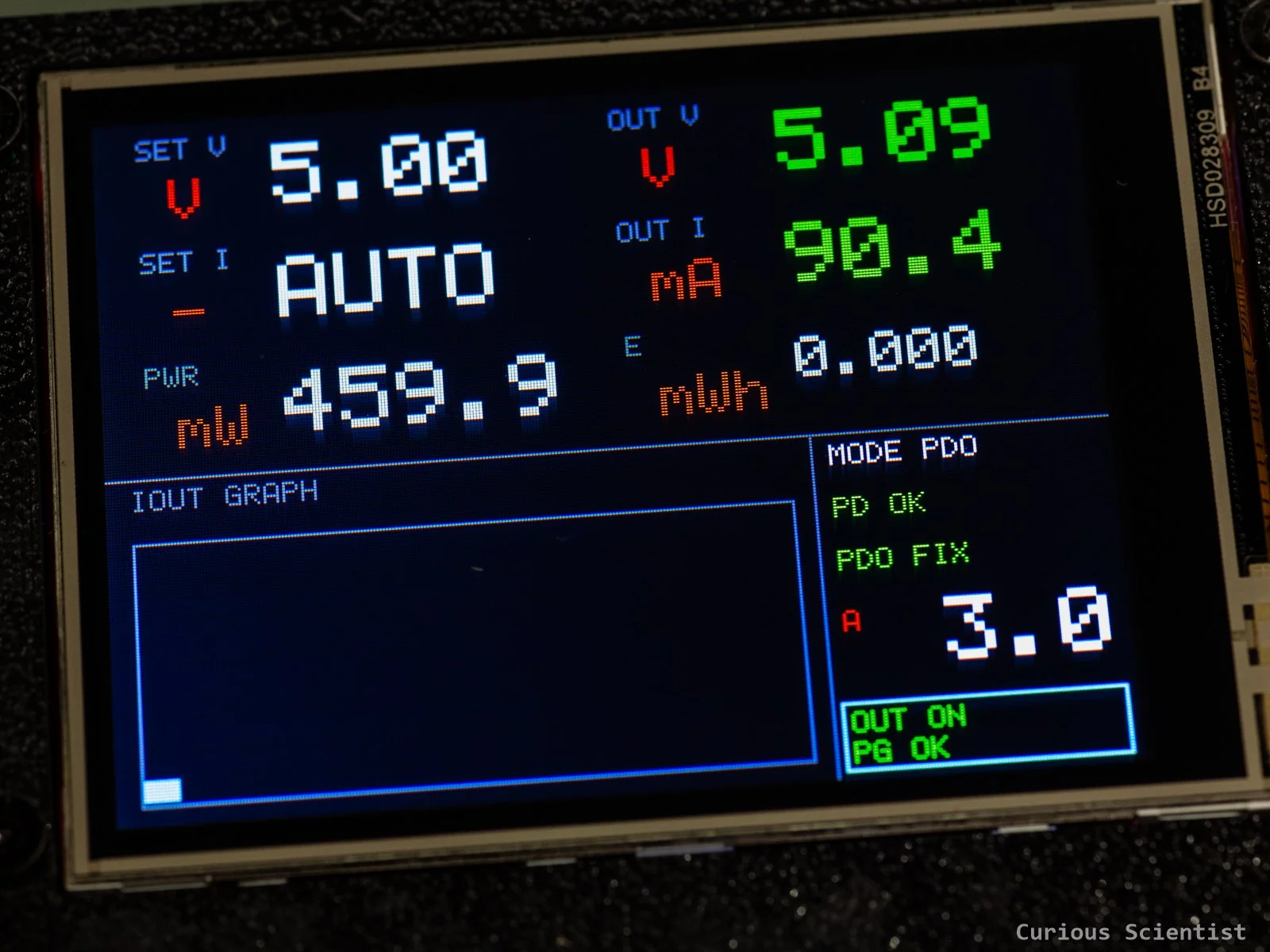
I tried to make the software as simple and as intuitive as possible. The 2.8” 320×240 display provides enough room for a proper user interface. Not only numbers and text, but even a small graph got some surface area on the display.
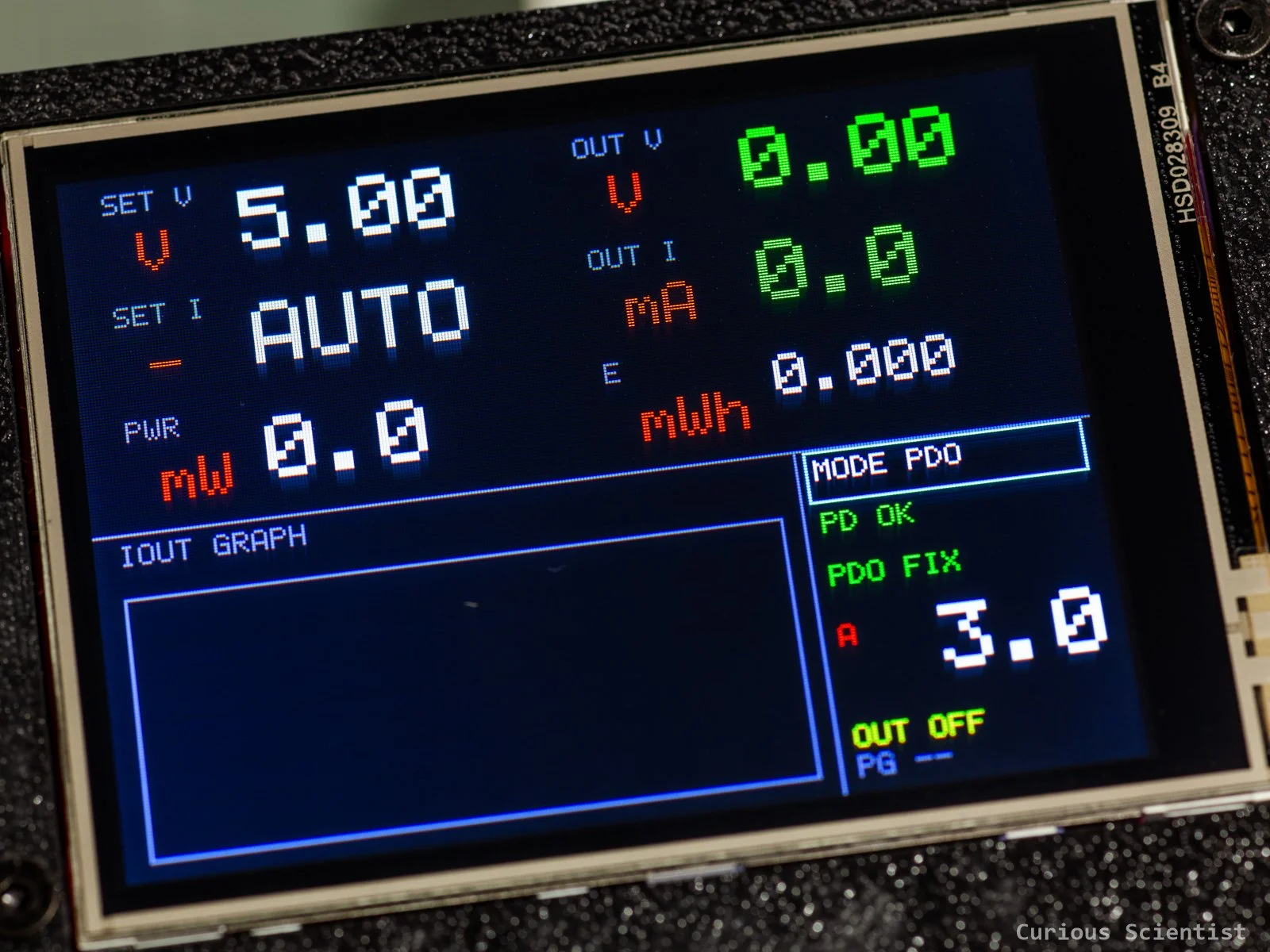
When the device is powered on, both the static and the dynamic parts are populated. The device starts in PDO mode, and it defaults to 5 V. The output is also disabled. The user can navigate on the display using the rotary encoder. Turning the encoder changes which active item is highlighted. To enter or exit edit mode, the user must press the switch of the encoder. Typically, the user can select (PDO mode) or adjust (PPS mode) the output voltage.
When in PDO mode, the user can select from a list of voltages, based on the power adapter’s capabilities. As mentioned before, these voltages are typically 5 V, 9 V, 12 V, 15 V and 20 V. In PDO mode, the maximum current is automatically set by the power supply’s capability, and it is shown on the display.
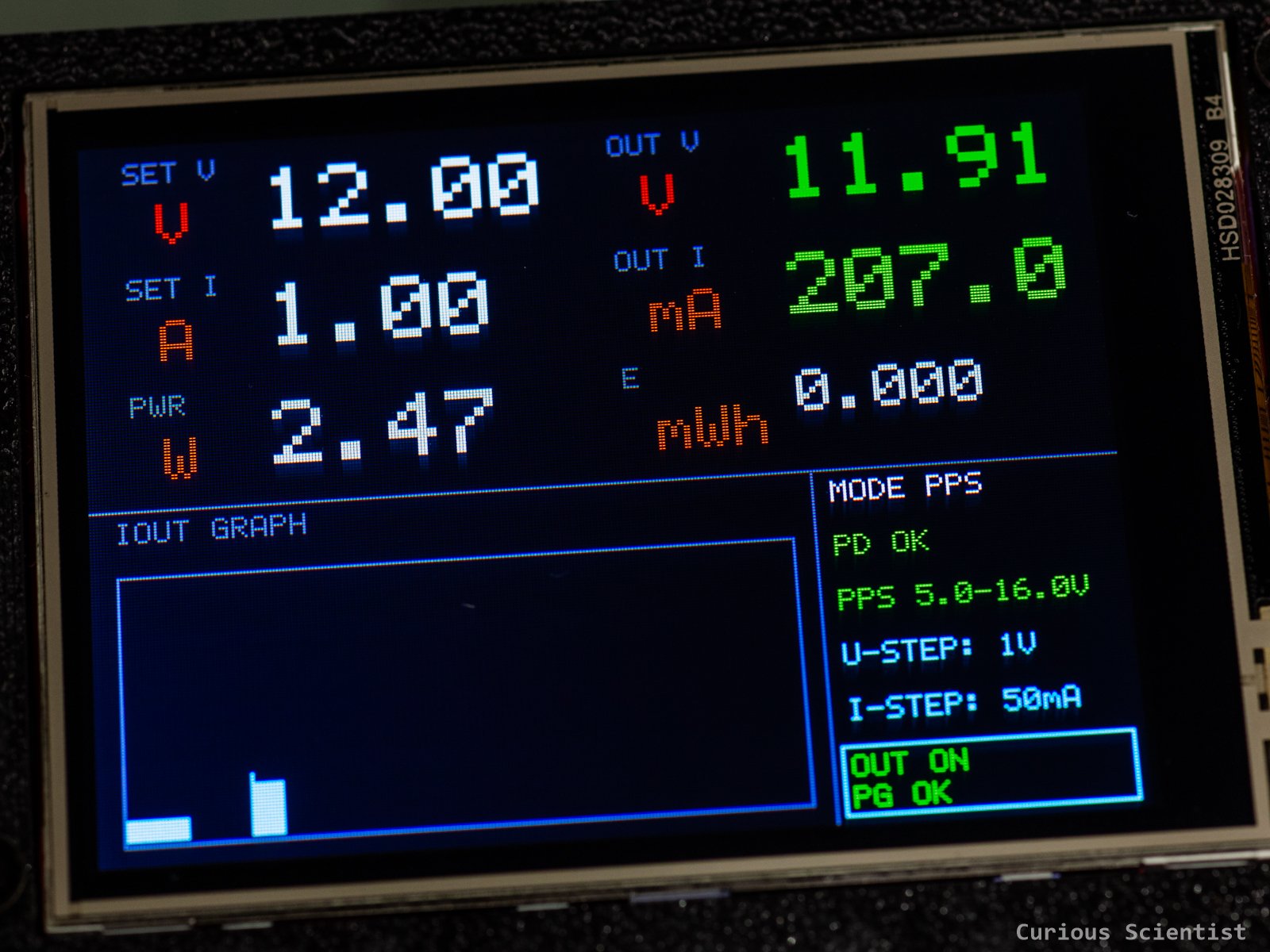
In PPS mode, the user can adjust the voltage (U-step) in 20 mV, 100 mV, 500 mV and 1 V steps, and can adjust the current limit in 50 mA, 100 mA, 200 mA and 500 mA steps. The set values can be anything within the power adapter’s capabilities. The voltage capabilities are shown on the display.
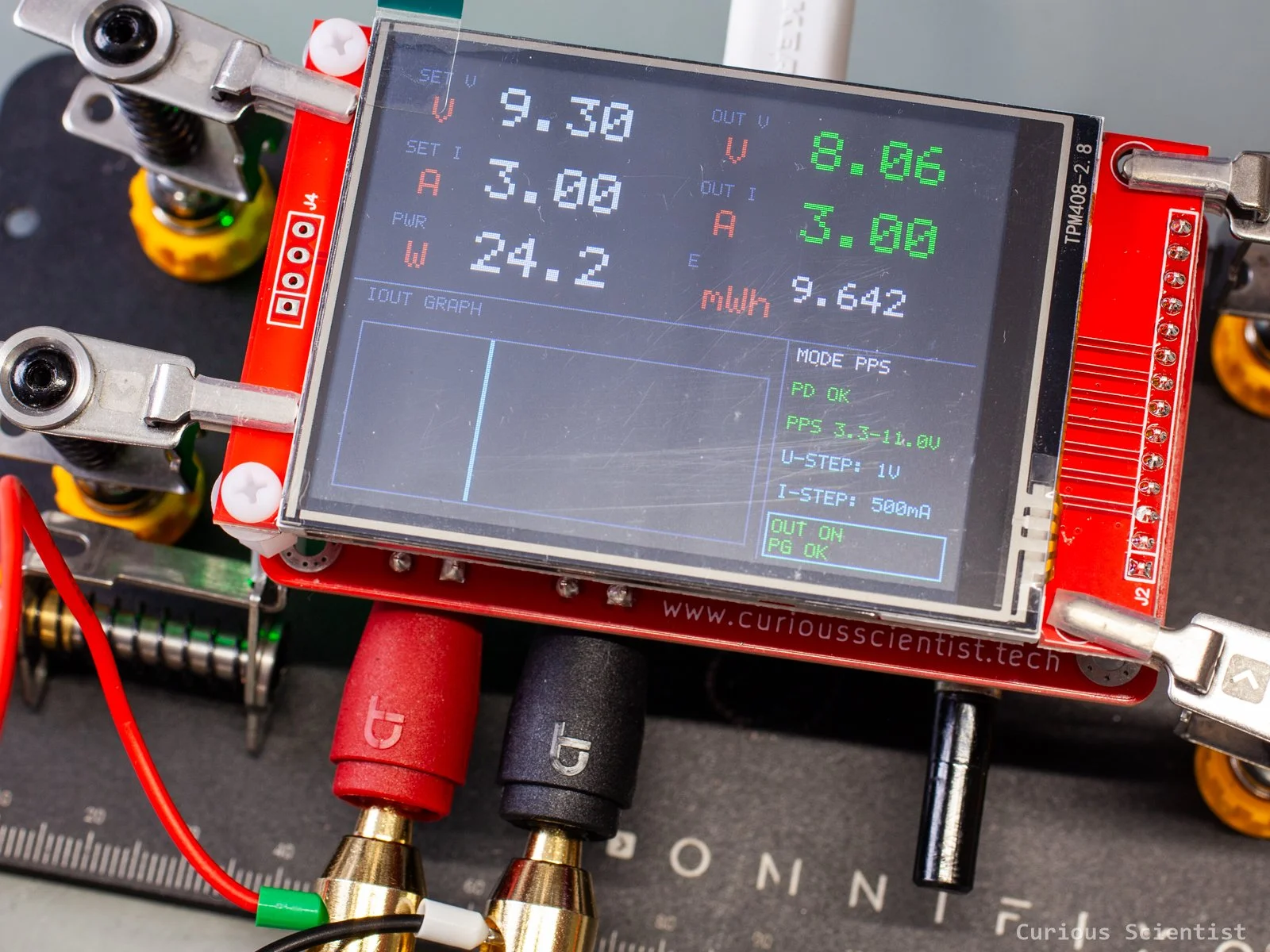
The set values, voltage and current, regardless of the active mode, are shown on the left side of the display. The output values are shown on the right side of the picture. Apart from the current and voltage, the device also provides power and energy values. These four values are derived from the measurements performed by the INA226 chip.
The output-related values are obviously zero as long as the output (ideal diode) is disabled. The user can navigate to the corresponding area on the display and turn the output on. Apart from the software ON/OFF status, the PG status of the ideal diode is also displayed on the display. When the output is enabled and the PG is good, the display prints “OUT ON PG OK”.
When there is current flowing through the output (so the current is not zero), the graph also prints the current. Each second, a vertical line is added to the display area, and based on the available pixels in the frame, the software can print roughly 3.5 minutes before the chart wraps around and starts over. The height of the vertical line is proportional to the current. The default Y-axis range is 1 A, but if the current jumps to, let’s say, 3 A, then the graph rescales itself to Y-max = 3 A.
Testing and results
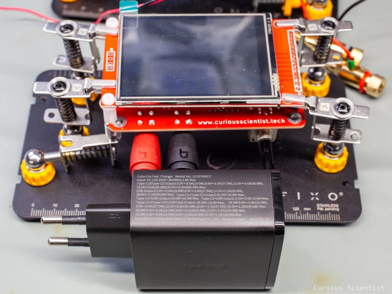
First of all, I could not test the capabilities of the circuit all the way up to 100 W because I only have a 65 W PD-capable power adapter. If anyone feels like donating $50 to me, I will immediately buy a charger and publish the results here. Until then, I publish the 65 W results.
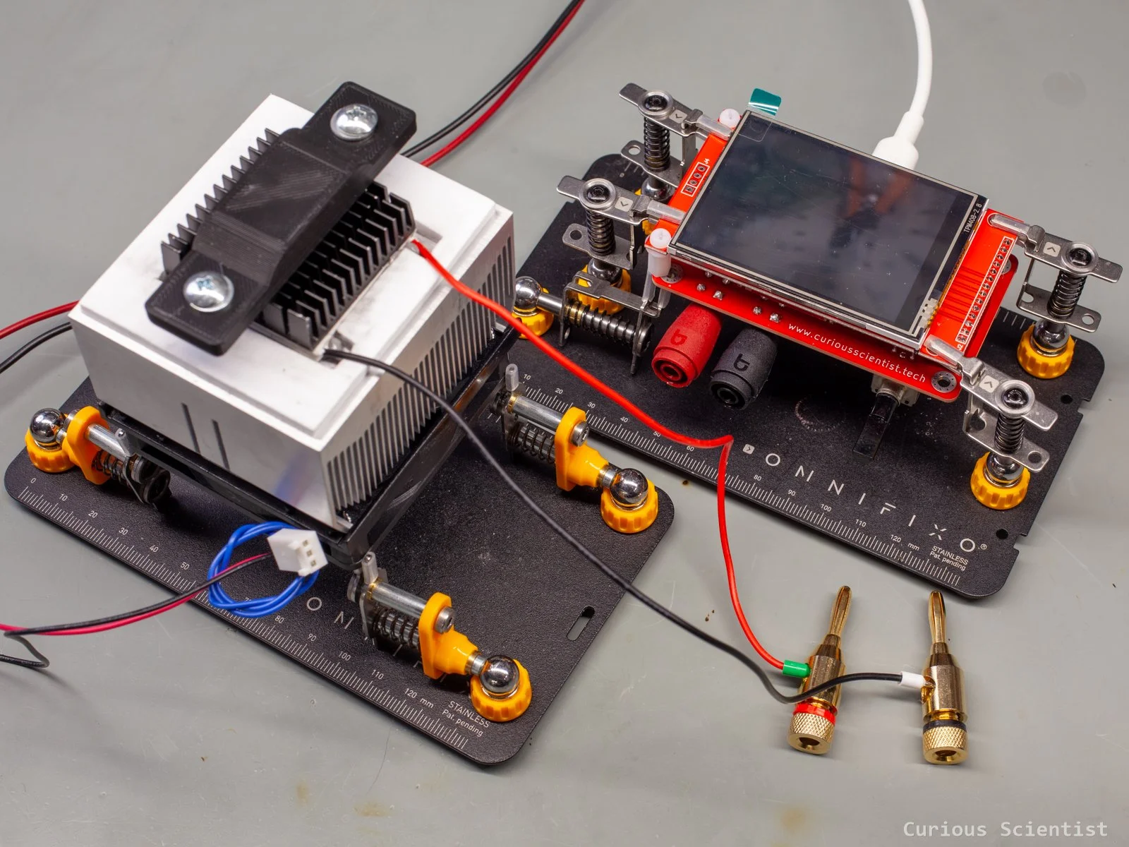
To get the maximum possible current draw, I used a TEC-12705 (5 A) Peltier cooler as the load. It is basically a high-power resistor that is easy to cool thanks to its relatively large flat surface. I mounted it on an old CPU cooler and clamped it down using a 4 cm x 4 cm heat sink.
First, I tested the device in PDO mode. At 5 V, the Peltier cooler drew about 1.6 A. This was nothing surprising. Then, I switched to 9 V, and I could reach 2.96 A. This is basically as high as my power adapter could go. I tried to operate the circuit at 12 V as well, but since that was over the adapter’s capabilities, I could not make it work properly. Of course, it was not my intention to operate the adapter outside of its “comfort zone”.
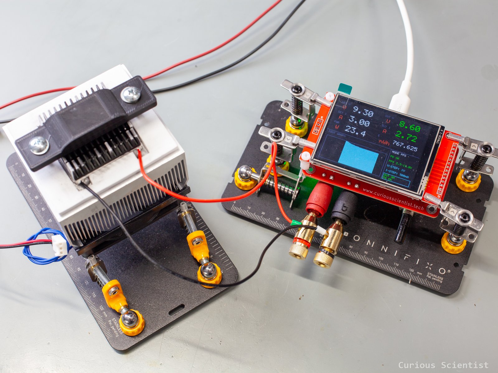
I switched to PPS mode and set the voltage slightly above 9 V (9.3 V) and ran it. The device was running at its maximum capability, 3 A. I could see that the voltage did not go all the way up to 9.3 V, but it stayed at around 8.5 V. I believe this is because the adapter was only able to provide 3 A and that 3 A was already reached at 8.5 V. I checked it with a benchtop power supply, and I could see that at 8.5 V, the current draw was 3 A, and at 9.3 V, it was 3.4 A.
I also tried running the device at 3.3 V. This was very important because this is one of the cornerstones of the whole hardware design. I wanted to be able to use the device even when it was receiving 3.3 V from the USB power supply, and this is why I added a buck-boost converter to the circuit. Luckily, even at this low voltage and under load, the board had no issues staying alive.
Additional content
Please consider using my AliExpress affiliate links for purchasing relevant gadgets!
Get the board from PCBWay!

If you found this content useful, please consider joining my YouTube channel’s membership or leaving a donation.
Also, please consider using my affiliate links when buying relevant gadgets.