ADS1256 + RP2040 Custom DAQ
In my last video on this topic, I said that I finished this product because I managed to make a proper connection between the front panel and the PCB using a flexible PCB. In the meantime, I have been searching for alternative and better solutions because the cost of manufacturing these flexible PCBs is not exactly cheap. So, I tried to find something off the shelf that is mass-produced and therefore cheap. In this article, I show you the solution I found, explain a bit more about the board and demonstrate its capabilities and performance. I will also talk about the official Arduino library I made for this chip because there have been some improvements done on it as well.
Introduction
For those who haven’t been following this project, I want to start with a short introduction.
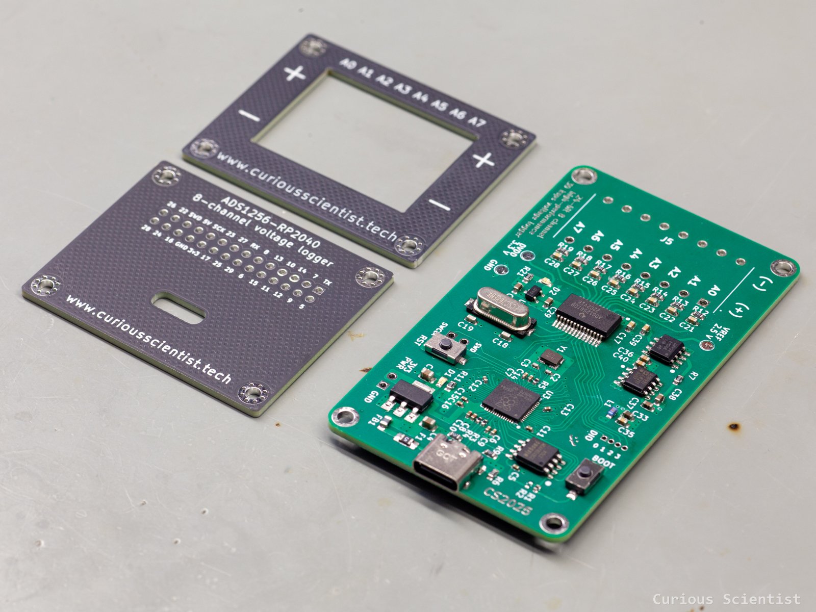
This is an 8-channel data acquisition (DAQ) board with a high-performance AD converter chip (ADS1256) and a high-performance microcontroller. The ADS1256 is an 8-channel, 24-bit analogue-to-digital converter chip that is capable of reaching up to 30kSPS output rates. It has fairly good performance, which makes it popular for projects that require multiple high-resolution channels. Originally, I developed this board with an ATmega32u4 microcontroller, but I quickly realised that despite its native USB, many GPIO ports and somewhat better performance than the “average Arduino board”, it can’t keep up with the ADS1256 at high sampling rates. Therefore, I transitioned the design to the RP2040. This is a much more powerful microcontroller with even more GPIOs, native USB support, a huge amount of (external) memory and more.
To ensure good performance, the ADS1256 receives its reference voltage from a buffered REF5025, a 2.5 V voltage reference chip. The buffering is provided by an OPA350 chip in, guess what, buffer/voltage follower mode. The ADS1256 has its own digital power supply (DVDD) provided by an XC6206P332MR voltage regulator.
The main circuit board has other convenient features such as easy access to the programming pins (SWCLK, SWD) of the RP2040 or the onboard 3.3 V line. Not the 3.3 V line of the ADS1256, but the separate one that feeds the rest of the circuit. There are also several test points on the circuit that allow the user to check the actual reference voltage value or to see if the 3.3 V for the ADS1256 is really 3.3 V.
Where it was possible or necessary, I used planes for power instead of just traces. This is especially valid around the USB supply and around the 3.3 V voltage regulator.
There are invisible features in the board as well. They are not visible because they are inside the board. This is because the board actually has four layers. On the top and the bottom layers, I run the signals and the power rails. I tried to separate them a bit, and for example, most of the 5 V lines are on the bottom side of the board; the 3.3 V and the voltage reference lines are on the top side. The two middle layers are both ground. This might not be accepted by some people, but after reading a lot of discussions on Stack Exchange and Reddit, it seems that the SIG/PWR-GND-GND-SIG/PWR layout is preferred by many people.
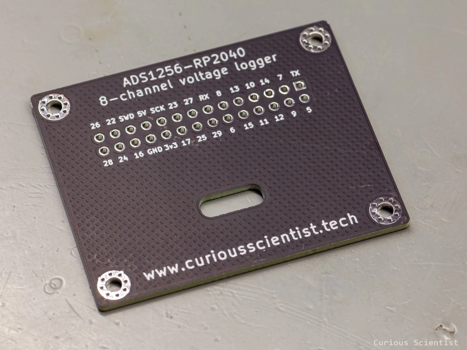
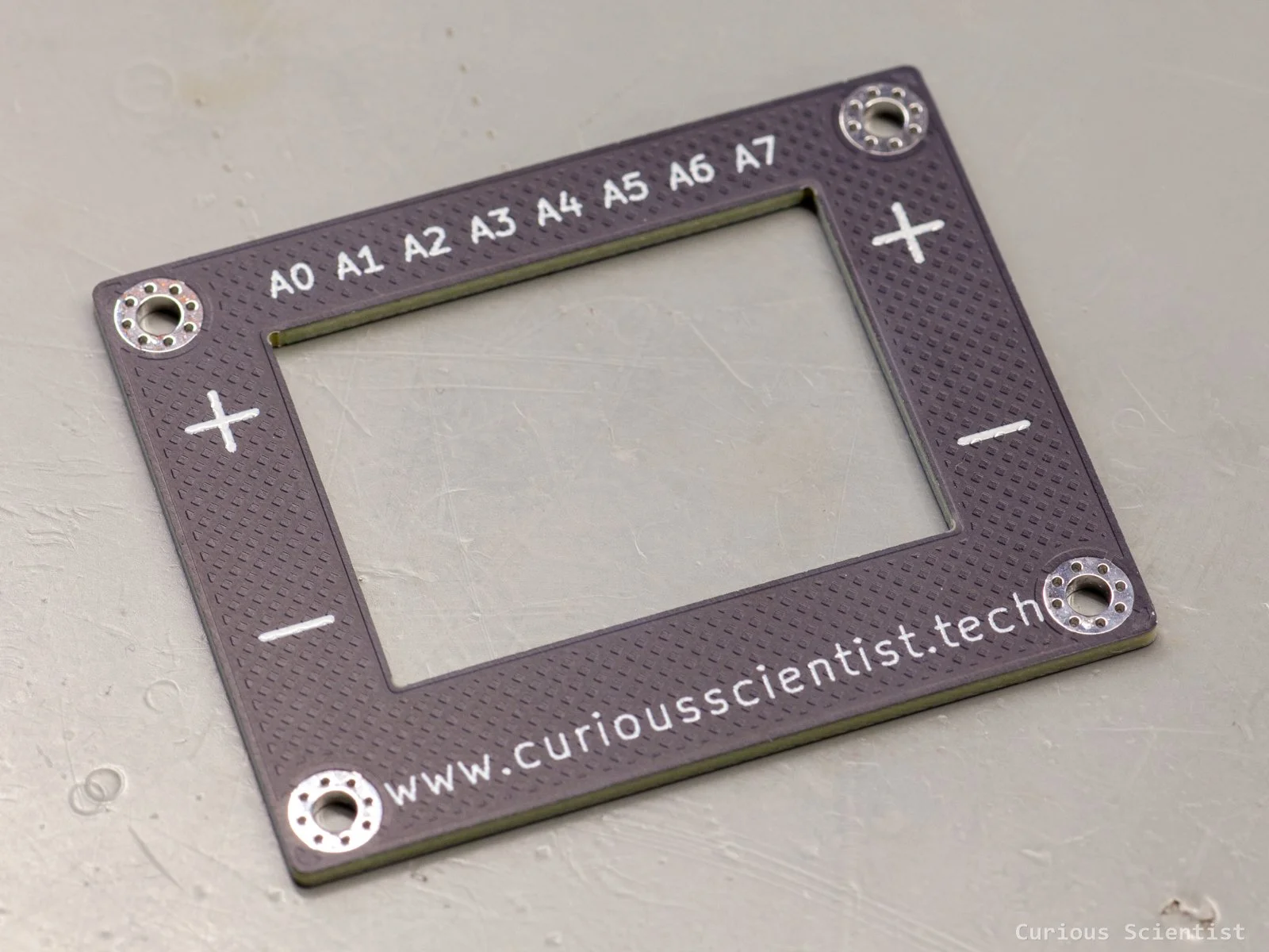
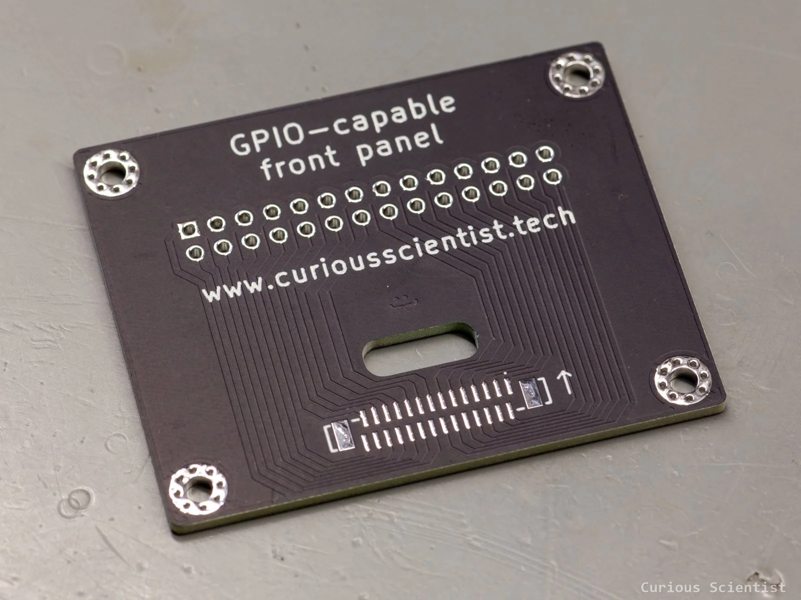
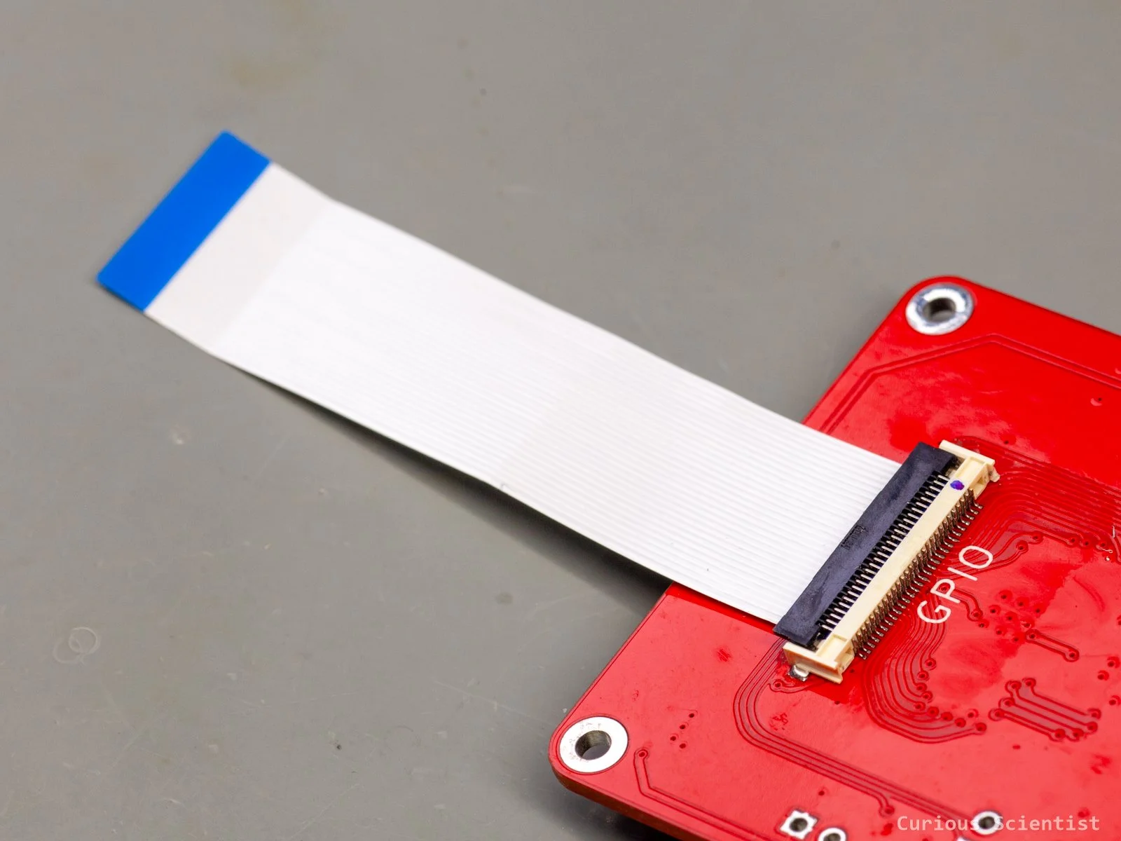
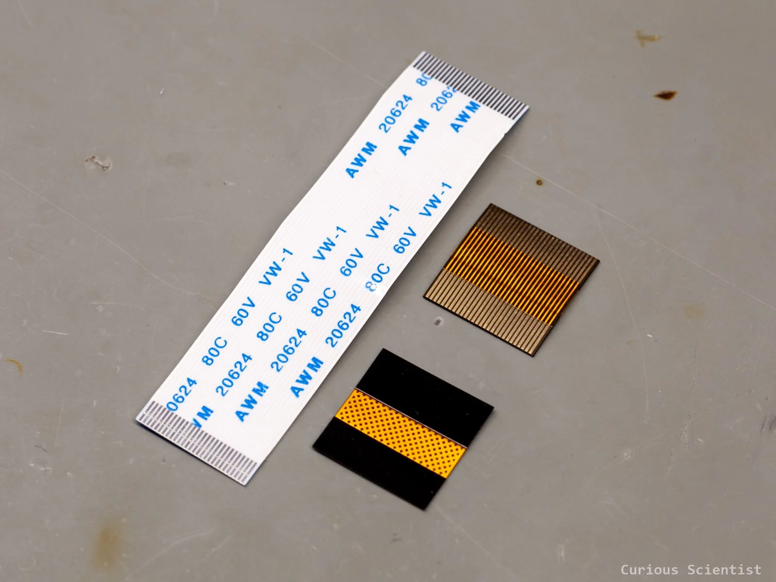
So, after hooking up the RP2040 with its external memory and the ADS1256, there are still 25 GPIOs left. They, and the three power pins: GND, 5 V and 3.3 V together, are 28 additional connections that can/must go somewhere. So, this started my initial work, where I made a front panel out of a PCB where one can access all these pins. But, at that time, I used a very cumbersome approach that needed a lot of very meticulous soldering and crimping. Then, some viewers suggested that I should look at some automotive connectors, and later, I ended up finally making the previously-mentioned flex PCB-based connector.
Now finally (and I swear), I settled with a solution. I found a short enough, off-the-shelf 28-pin flexible ribbon cable that fits the already existing connector on the main PCB. Furthermore, I found a much cheaper socket for the front panel on AliExpress as well. The only problem was that I had to reroute the front panel because the socket was mirrored compared to the originally used one. So, some of my earlier front panels don’t work with this cheaper type of connector.
With these changes, I finally dare to say that this project is finished, and I think it is mature enough to become a product.
Demonstration
To test whether the front panel works as it should, I did a very simple experiment. I wrote a short code that reads all the GPIOs that were made available on the front panel. It is just a simple digitalRead() function. Then, with the help of a small resistor (4.7k) I shorted the pins to 3.3 V one by one. When the shorted pin was recognised by the code, it printed the corresponding port number on the serial terminal. It was a bit tedious to go through all 25 pins, but it is part of the quality check process.
Thanks to the fact that the RP2040 has a very flexible way of handling the GPIOs, we have access to many extra features via the front panel pins. They are not only GPIOs, but they can be used as SPI, I2C or serial peripherals as well. In my earlier video, I already demonstrated this by connecting a display to the front panel and displaying some measurement data on it.
With a bit more flexible thinking, we can turn this DAQ into a remote logger by adding not only a display, but also some buttons and an SD card reader.

The earlier iteration of the GPIO front panel could already drive external devices.
Also, since the last video on this circuit, the Arduino library for the ADS1256 chip has gone through a lot of improvements.
For example, the SPI communication part of the library has been entirely reworked. This allows the user to assign any of the SPI peripherals of the microcontroller to the ADS1256. Previously, this was only possible by modifying the library, but now, the user can do it by just updating a few lines in the provided example code. All the SPI configuration-related lines are carefully documented in the library’s documentation, including the microcontroller-specific parts. I carefully tested the library with at least 10 different microcontrollers, such as Teensy 4.0, different ESP32 models, Arduino Uno, Nano and Mega, STM32 “blue pill” (F103C8T6) and “black pill” (F401CCU6) and so on. These boards are also in the example code with the necessary pin definitions and so on.
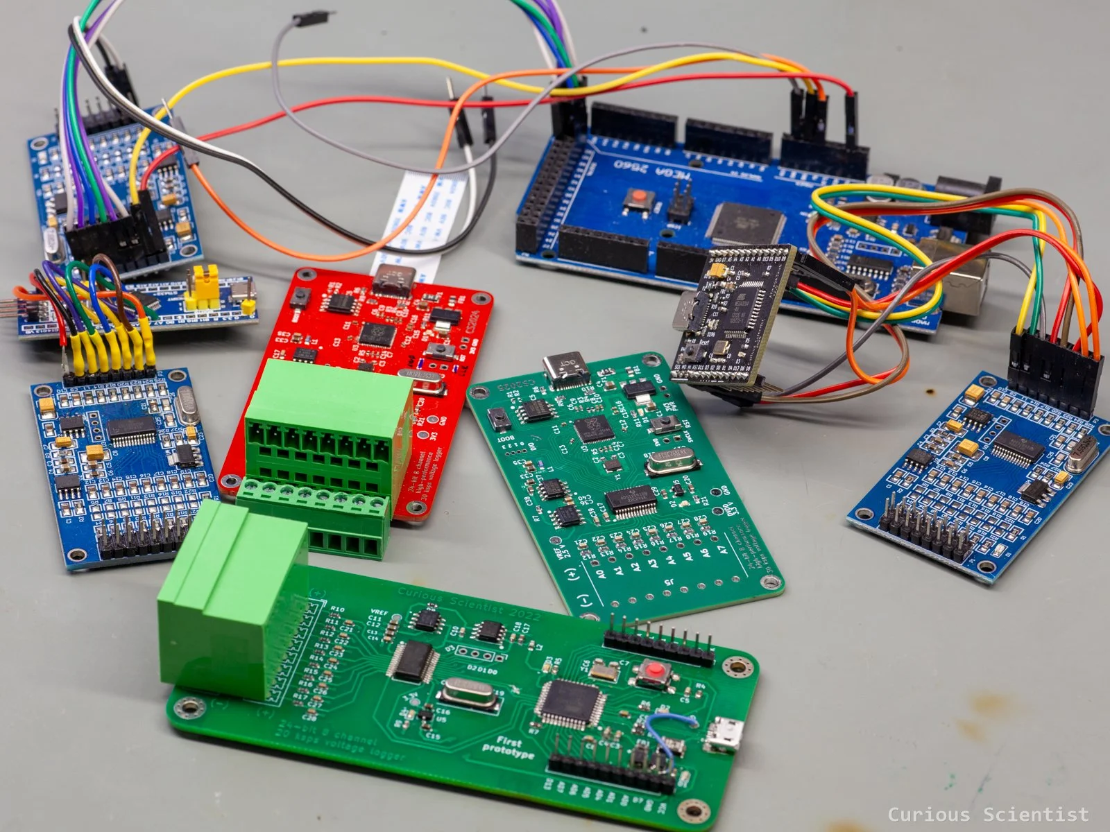
A few, but not all the MCUs that have been (successfully) tested for my ADS1256 Arduino library
Performance
Finally, let’s have a series of tests that demonstrate the capabilities of my board with the ADS1256 chip and the REF5025 voltage reference.
Noise floor test
In this test, I just shorted AIN+ and AIN- (A0 and A1) together and connected them to GND. Then I set the input to [A0+A1] differential input, set PGA = 1, and set the sampling rate to 100 SPS and collected 10000 samples.
The results are the following:
| Parameter | Value |
|---|---|
| Data Rate | 100 SPS |
| Samples | 10000 |
| Mean | -14.443 counts / -8.344 µV |
| Minimum | -22 counts |
| Maximum | -7 counts |
| Peak-to-peak noise | 15 counts / 8.940 µV |
| RMS noise | 1.865 counts / 0.596 µV |
To see if decreasing the sampling rate helps with the noise, I performed the same experiment with 10 SPS. The board achieved a peak-to-peak noise of only 3.6 uV and an RMS noise of approximately 0.46 uV.
| Parameter | Value |
|---|---|
| Data Rate | 10 SPS |
| Samples | 10000 |
| Mean | -12.218 counts / -7.152 µV |
| Minimum | -15 counts |
| Maximum | -9 counts |
| Peak-to-peak noise | 6 counts / 3.576 µV |
| RMS noise | 0.766 counts / 0.456 µV |
A rough estimate for the noise-free bits is about 21.4 bits at 10 SPS and PGA = 1. This is based on the 10 V range of the ADC (-5 V to +5 V) and the peak-to-peak noise of 3.576 uV.
Just as a comparison, the datasheet (Table 3) reports 22.3 noise-free bits at 10 SPS and PGA=1. Not too bad, I guess.
void runADCNoiseTest()
{
    const uint32_t samples = 100;

    long value;
    long minValue = 2147483647;
    long maxValue = -2147483648;

    double sum = 0;
    double sumSquares = 0;

    Serial.println();
    Serial.println("ADS1256 noise test started");
    Serial.println("Input should be shorted: AIN0 + AIN1 + GND");
    Serial.println();

    A.setMUX(DIFF_0_1);
    A.setPGA(PGA_1);
    A.setDRATE(DRATE_10SPS);

    delay(1000);

    for (uint32_t i = 0; i < samples; i++)
    {
        value = A.readSingle();

        if (value < minValue) minValue = value;
        if (value > maxValue) maxValue = value;

        sum += value;
        sumSquares += (double)value * (double)value;
    }

    double mean = sum / samples;

    double variance = (sumSquares / samples) - (mean * mean);
    double rmsNoiseCounts = sqrt(variance);

    long peakToPeakCounts = maxValue - minValue;

    double meanVoltage = A.convertToVoltage(mean);
    double rmsNoiseVoltage = A.convertToVoltage(rmsNoiseCounts);
    double peakToPeakVoltage = A.convertToVoltage(peakToPeakCounts);

    Serial.println("ADS1256 noise test finished");
    Serial.println("---------------------------");

    Serial.print("Samples: ");
    Serial.println(samples);

    Serial.print("Mean [counts]: ");
    Serial.println(mean, 3);

    Serial.print("Min [counts]: ");
    Serial.println(minValue);

    Serial.print("Max [counts]: ");
    Serial.println(maxValue);

    Serial.print("Peak-to-peak [counts]: ");
    Serial.println(peakToPeakCounts);

    Serial.print("RMS noise [counts]: ");
    Serial.println(rmsNoiseCounts, 3);

    Serial.println();

    Serial.print("Mean [V]: ");
    Serial.println(meanVoltage, 9);

    Serial.print("Peak-to-peak noise [V]: ");
    Serial.println(peakToPeakVoltage, 9);

    Serial.print("RMS noise [V]: ");
    Serial.println(rmsNoiseVoltage, 9);

    Serial.println("---------------------------");
}
Reference voltage measurement
I have an AD584-M voltage reference circuit. I measured its 2.5 V output using all the single-ended channels (SING_0 → SING_7) and all the differential channel pairs (DIFF_0_1 → DIFF_6_7).
The results are the following:
| Test | Mean Voltage | Error | Error % | Pk-Pk Noise | RMS Noise |
|---|---|---|---|---|---|
| SING_0 | 2.499001 V | -0.999 mV | -0.0399% | 20.264 µV | 2.384 µV |
| SING_1 | 2.499008 V | -0.992 mV | -0.0397% | 16.688 µV | 2.384 µV |
| SING_2 | 2.499016 V | -0.984 mV | -0.0393% | 20.860 µV | 2.384 µV |
| SING_3 | 2.499018 V | -0.982 mV | -0.0393% | 21.456 µV | 2.980 µV |
| SING_4 | 2.499020 V | -0.980 mV | -0.0392% | 16.092 µV | 2.384 µV |
| SING_5 | 2.499017 V | -0.983 mV | -0.0393% | 17.284 µV | 2.384 µV |
| SING_6 | 2.499019 V | -0.981 mV | -0.0393% | 14.900 µV | 2.384 µV |
| SING_7 | 2.499014 V | -0.986 mV | -0.0394% | 22.052 µV | 2.384 µV |
| DIFF_0_1 | 2.497985 V | -2.015 mV | -0.0806% | 24.435 µV | 4.172 µV |
| DIFF_2_3 | 2.498091 V | -1.909 mV | -0.0764% | 34.567 µV | 7.152 µV |
| DIFF_4_5 | 2.498108 V | -1.892 mV | -0.0757% | 36.355 µV | 7.748 µV |
| DIFF_6_7 | 2.498134 V | -1.866 mV | -0.0746% | 40.527 µV | 6.556 µV |
As we can see, the single-ended measurements are remarkably consistent. The differential channels are not that consistent and they report a slightly different value as well. This could be due to several reasons. The single-ended and the differential measurements require different input paths. This essentially doubles the contribution of input leakage, source impedance effects, settling errors…etc. Also, if there’s an imperfection in the common-mode rejection, the differential mode picks it up. Furthermore, source impedance imbalance can also occur due to the fact that while AIN+ was directly connected to the source, AIN- was connected to the ground and these two nodes might have different impedance. Also, initially, the performance was somewhat worse in the beginning. So much worse that I disassembled the enclosure and cleaned the board. As it turned out, the flux residue “showed up” in the measurements and offset the A0 input significantly. Probably the cleaning is still not sufficient because the DIFF_0_1 channel still shows a noticeably lower value than the others.
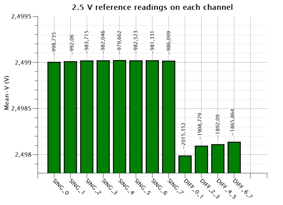
The height of the chart represents the absolute readings in Volts, and the numbers above the columns represent the absolute error in microVolts.
This area of the ADS1256 is extremely sensitive to contamination. Make sure to carefully clean up all the flux residues!
PGA gain comparison
I used a small signal from the same AD584-M reference I used above by dividing its 2.5 V output with a 100k:1k resistor ladder, and applied different PGA (gain) values to see how the board can resolve tiny signals at different gain settings. The signal should be roughly 25 mV, which is ideal for testing all PGA settings between 1 and 64. At PGA = 64, the highest measurable signal is 78.125 mV, so the expected ~25 mV is well within this range.
The results are the following:
| PGA | Mean Voltage | Mean Counts | Pk-Pk Noise | RMS Noise |
|---|---|---|---|---|
| PGA_1 | 24.322819 mV | 40,811 | 42.315 µV | 10.728 µV |
| PGA_2 | 24.323711 mV | 81,625 | 30.097 µV | 9.536 µV |
| PGA_4 | 24.321180 mV | 163,234 | 30.395 µV | 12.665 µV |
| PGA_8 | 24.318125 mV | 326,426 | 28.309 µV | 9.983 µV |
| PGA_16 | 24.312016 mV | 652,687 | 37.882 µV | 11.138 µV |
| PGA_32 | 24.308532 mV | 1,305,185 | 36.430 µV | 12.516 µV |
| PGA_64 | 24.308644 mV | 2,610,383 | 29.315 µV | 12.153 µV |
The difference between PGA_1 and PGA_64 is tiny, only about 14 uV. So, the measured voltage stays almost constant from PGA_1 to PGA_64. This means that the PGA scaling works correctly.
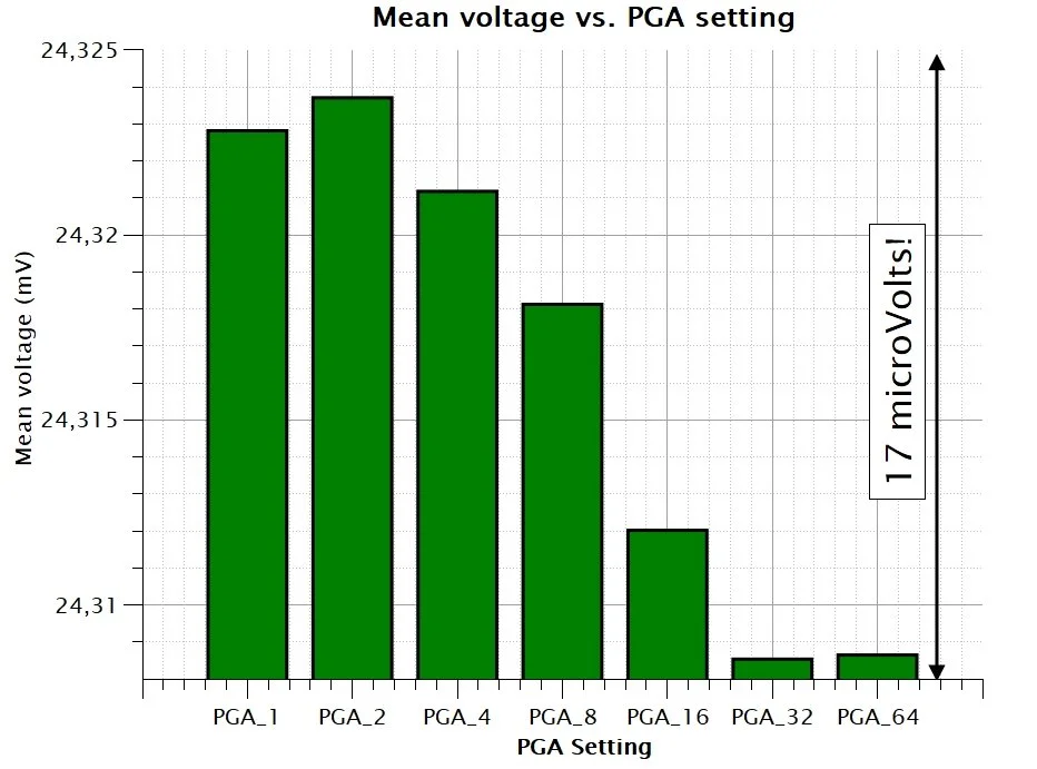
It is worth noting that the shown distance along the Y-axes is only 17 uV!
Data rate vs noise test
I used the same voltage reference circuit as before and measured its output at different sampling rate values.
| Data Rate | Samples | Mean | Pk-Pk Noise | RMS Noise |
|---|---|---|---|---|
| 30000 SPS | 10000 | -14.696 counts / -8.344 µV | 313 counts / 186.544 µV | 29.134 counts / 17.284 µV |
| 7500 SPS | 10000 | -26.423 counts / -15.496 µV | 136 counts / 81.054 µV | 17.524 counts / 10.132 µV |
| 1000 SPS | 10000 | -10.240 counts / -5.960 µV | 52 counts / 30.991 µV | 6.768 counts / 3.576 µV |
| 100 SPS | 10000 | -12.795 counts / -7.152 µV | 16 counts / 9.536 µV | 2.100 counts / 1.192 µV |
| 10 SPS | 1000 | -12.623 counts / -7.152 µV | 6 counts / 3.576 µV | 1.027 counts / 0.596 µV |
| 2 SPS | 1000 | -11.634 counts / -6.556 µV | 4 counts / 2.384 µV | 0.839 counts / ~0.500 µV |
As we can see, decreasing the sampling rate greatly improves the noise performance. The measurement confirms the practical tradeoff described in the datasheet: the ADS1256 can be configured either for high-speed measurements or for lower-noise, higher-resolution measurements by changing the digital filter setting through the DRATE register.
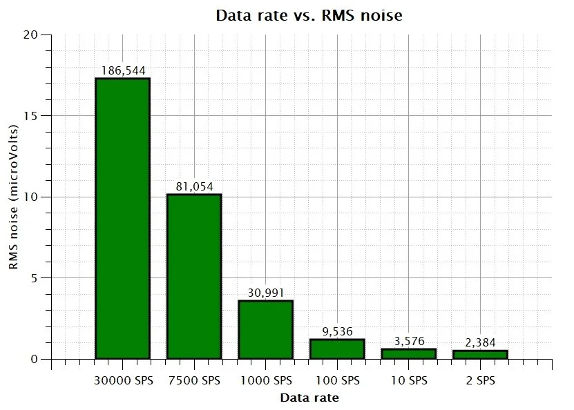
The height of the columns represents the RMS noise, and the numbers above the columns represent the peak-to-peak noise in microVolts.
Differential polarity verification
Since the ADS1256 can perform true bipolar differential measurements, I wanted to test it as well. I used the same resistor-divided 2.5 V voltage reference (~25 mV output) as I used in one of the earlier tests. I connected the output of the divider to A0 and the GND to A1. I measured 1000 samples at 100 SPS data rate and evaluated the noise parameters. Then I flipped the wires so that A1 measured the output of the resistor divider and A0 was connected to GND, and I measured the same parameters.
The original wiring gave about 24.31 mV, and after reversing the connections, the value changed to approximately -24.32 mV. I repeated the test several times, and the difference between measurements remained within 10-15 uV. This shows good symmetry and repeatability.
"Real-life” demo with a load cell
I connected the output of a 100 g load cell directly to the input of the board to show how it works. The excitation voltage was provided by the previously used AD584-M chip at 5 V. Then, as the table below shows, I applied different loads and read the corresponding counts. The data rate was set to 10 SPS, and the PGA was set to the highest value: 64. 20 Samples were collected through the A0+A1 differential input.
| Load | Mean Counts | Net Counts | RMS Noise | Mean Voltage |
|---|---|---|---|---|
| 0 g | -10055.070 | 0 | 57.627 counts | -93.635 µV |
| 10 g | 24738.500 | 34793.570 | 9.929 counts | 230.368 µV |
| 20 g | 59216.370 | 69271.440 | 10.849 counts | 551.437 µV |
| 50 g | 162833.770 | 172888.840 | 10.323 counts | 1516.349 µV |
| 100 g | 335326.440 | 345381.510 | 25.279 counts | 3122.654 µV |
| 0 g repeat | -9558.480 | 496.590 | 8.764 counts | -89.007 µV |
The measured data points were plotted with the applied weight (grams) on the X-axis and the corresponding mean ADC counts on the Y-axis. A linear fit was then applied to the dataset. The slope of the fitted line (parameter A) represents the sensitivity of the system in counts per gram, while the intercept (parameter B) represents the zero-offset count value.
By rearranging the linear equation and substituting the measured ADC counts, the applied weight can be calculated directly in grams. The resulting calibration curve showed good linearity over the tested range of 0 to 100 grams. This demonstrates the suitability of the ADS1256 and load-cell combination for precision weighing applications.
It is worth noting that the calibration parameter A remains fixed once a calibration procedure has been performed; however, the zero-offset value can be updated at any time by taring the scale. This is important because updating the zero-offset removes errors caused by load-cell drift, the mounting hardware, temperature changes, and other environmental influences. As a result, the scale can maintain accurate measurements without requiring a complete recalibration. Only the reference point is adjusted, while the sensitivity of the system (counts per gram) remains unchanged.
Additional content
Support me by using these affiliate links
2×8 pin screw terminal connector
Get the 2-layer* PCB from PCBway!

*My 4-layer PCB with the FPC connector and front panel are not shared on purpose. If you want one of those, contact me using the contact form on my website.