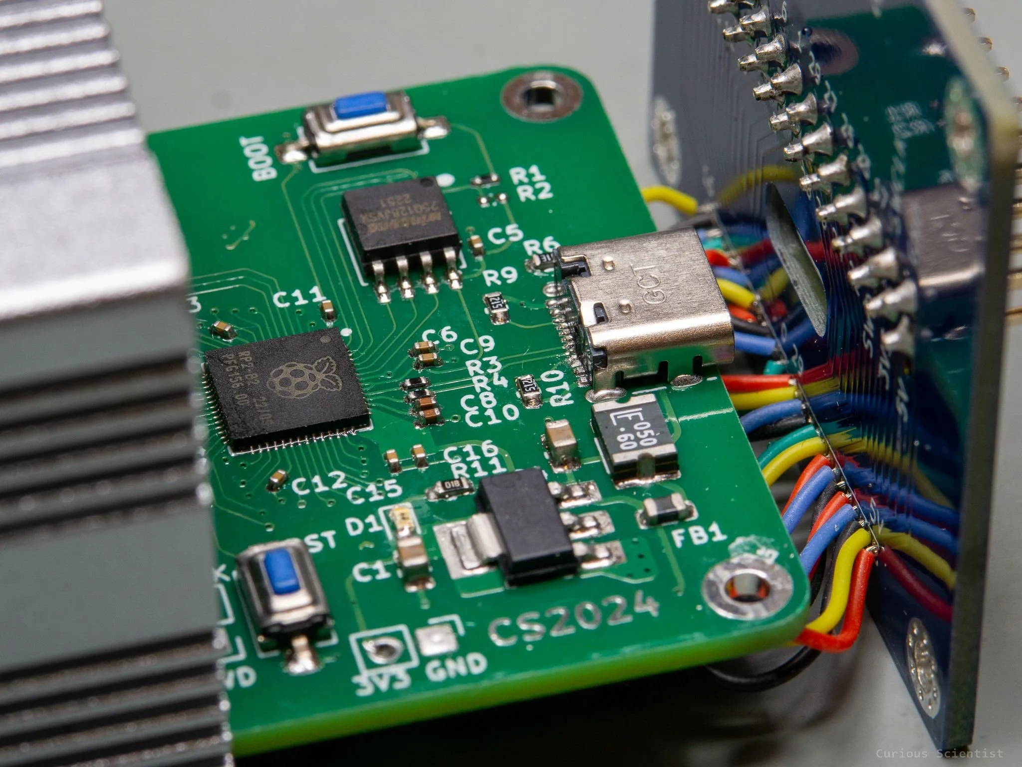
ADS1256-RP2040 circuit with GPIO front panel - Finished!
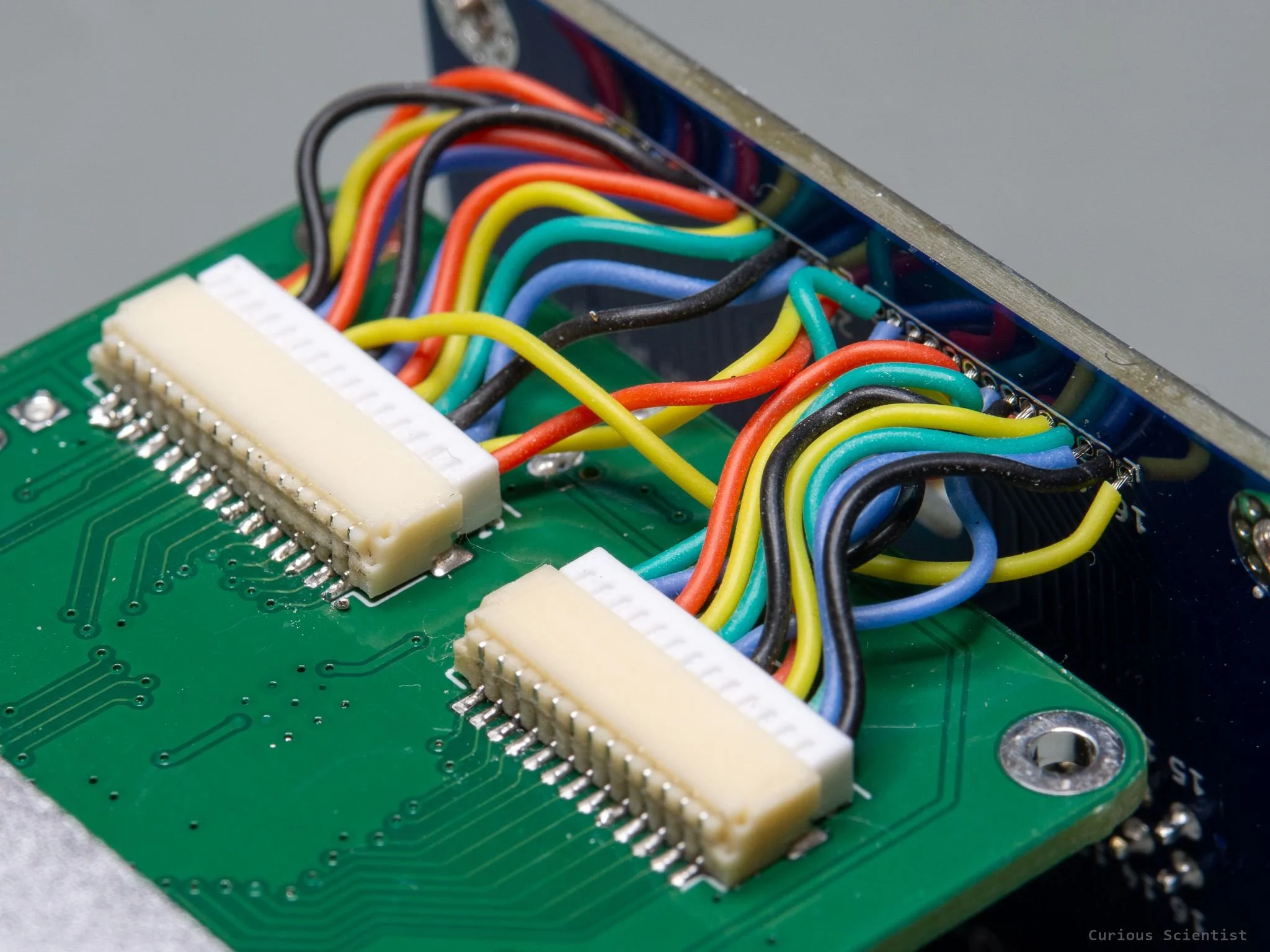
In this video, I show you the finished project regarding my ADS1256-RP2040 circuit with a PCB-based front panel. Previously, I already introduced two PCB-based front panel designs. One without any GPIO pins and another with all the available GPIO pins of the RP2040. Unfortunately, I could not finish the GPIO project to 100% because I could not crimp those tiny JSH SH 1.0 connectors properly. But now I have all the parts and tools for the task, so I finished the project and built everything.
Additional information and resources
So, the task was not super difficult with the pre-crimped wires. I just had to cut the wires to the correct length, strip off 2-3 mm insulation from them, insert them in the plastic housing and then solder them one-by-one to the GPIO front panel. The soldering was a bit tricky, because of the pitch of the holes for the cables. It was a bit hard to avoid shorting the connections together. But I did not care too much during the process, I just wanted to get all the wires sitting in their corresponding terminals. Once everything was tacked (soldering is a too good expression here), I flipped the front panel, added some flux and cleaned up all the connections. To be 100% sure, I measured the adjacent terminals with a multimeter to detect short circuits. There was none after the cleanup.
To demonstrate a use case of the GPIO front panel, I connected an i2C LCD to it. I wrote a few lines of code to the example I made for my ADS1256 Arduino library (link) and printed the voltages on the four differential input channels of the ADC. In the video, I compared the readings of the ADS1256 to a multimeter. Both devices measured the same voltage within a few milliVolts, which is good-enough for me. I did not apply any filtering or averaging on the values read by the ADS1256 and I used the largest PGA value, so the readings were “rough”, but still within tolerance when I compared them to the readings of the multimeter.
Get the relevant parts from my affiliate links!
Join my YouTube membership!
Get the PCBs from PCBWay!