CS1237 24-bit AD Converter with Arduino
In this video and article, I show you how you can work with the CS1237 24-bit AD converter using an Arduino-compatible microcontroller. I implemented a code from scratch that utilizes all the features of the ADC except the sleep mode because I don’t need sleep mode for my applications. Read the article below because I explain the chip in detail. This could be particularly useful because the datasheet of the ADC is in Chinese.
The ADC and its operation

“Test rig” for the CS1237 24-bit ADC. I used this simple circuit to develop the code for the chip. I picked an RP2040 Zero as the microcontroller due to its small footprint and its relevance for future projects.
I use this module with a built-in voltage reference chip that allows the module to be used with load cells in a ratiometric measurement mode. In ratiometric measurement, the output of the load cell, which is proportional to the applied force or weight, is compared to the reference voltage provided by the ADC. Since both the excitation voltage of the load cell and the reference voltage of the ADC are derived from the same source (such as the same power supply or voltage reference), variations or fluctuations in the supply voltage affect both the excitation voltage and the reference voltage proportionally. As a result, these variations cancel out, improving the accuracy and stability of the measurement. The voltage reference chip is there to provide both the VREF for the ADC and the excitation voltage for the load cell (or bridge). It is worth noticing, that the CS1237 has its own internal VREF, and it can be used by providing the correct values to the config register and shorting pin 1 to pin 8. The boards I use have the possibility to close a solder bridge to short pin 1 to pin 8.
When it comes to the module, we know the following things about it. The module has only two communication pins, a clock (SCLK) and a data (DRDY/DOUT) pin. The DRDY/DOUT pin is bidirectional which means that we can use it for both sending data to the module and reading from it. We send data to the module when we modify the config register and we read data from it when we read the config register or we acquire data.
The config register
The config register holds 8 bites (1 byte). The bits are the following:
Bit 0-1: Channel select
Bit 2-3: PGA select
Bit 4-5: SPEED select
Bit 6: VREF on/off
Bit 7: Reserved, not in use
This ADC actually has only one (differential) input channel, however, the user can also monitor the internal temperature of the chip, or can short the input pins (presumably for offset calibration). The PGA (Programmable Gain Amplifier) has 4 settings. 1, 2, 64 and 128. Similarly to the PGA settings, there are 4 acquisition speed settings as well: 10 Hz, 40 Hz, 640 Hz and 1280 Hz. Finally, there is one more bit left which could be relevant for the user which is the bit (bit 7) that sets the internal voltage reference (VREF) on or off.
Data acquisition
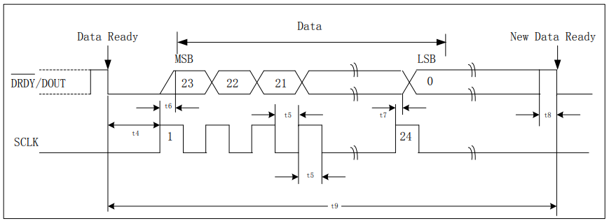
Timing of the shifting out of the 24-bit conversion. MSB shifted out first.
Before showing how to read or write the config register, let’s see how to acquire data. I chose to introduce the chip’s function in this way because the config register is accessed after data acquisition.
First, the DRDY pin has to go low. Then, within t4 time, we can start stepping out the data by providing a clock pulse. The simple thing about this chip is that we can simply toggle a GPIO pin to generate the SCLK pulses and then read out the bits from the DOUT pin with each SCLK pulse.
After shifting out all 24 bits, we have the acquisition data.
By providing SCLK pulses and reading DOUT at the 25th pulse, we can see if the config register was updated in the previous loop of reading data from the chip. The 26th and 27th pulses are kind of irrelevant to us, but we need to keep providing these pulses if we want to read or write the config register.

Timing of the acquisition and the reading of the config register. Notice that the input and output texts in the parentheses next to the DRDY texts represent the behaviour of the DRDY pin on the CS1237 chip!
Reading the config register
To read the register, we keep pulsing SCLK after the 27th pulse. We need to provide 2 additional pulses (pulses 28 and 29). Then we set the DOUT/DRDY pin on the microcontroller as an OUTPUT.
Then, in the next 8 pulses (pulses 30-36) we shift in the read command (0x56) to the CS1237 via the DOUT chip.
After finishing sending the command, we send one more pulse (37) and then switch the DOUT/DRDY pin on the microcontroller to become an INPUT because in the next eight pulses (38-45) we shift out the response from the CS1237 chip. The response is the content of the config register.
Finally, we send one more SCLK pulse to the chip.

A read request being sent to the CS1237. The signal is recorded by a logic analyzer. First, the 24-bits are shifted out. Then 3+2 dummy pulses are generated. Then the binary equivalent of 0x56 (read command) is shifted in. Then after the single clock pulse, the answer (content of the config register) is shifted out.

Timing of the acquisition and the reading of the config register. During the whole operation, up until the 46th pulse, the DOUT/DRDY pin stays output on the microcontroller. First we send the write command, then we send the data to the config register.
Writing to the config register
To write the register, we almost do the same as we do with reading. We do a reading, then we do 3 additional SCLK pulses. After the 27th pulse, we make sure that the DOUT/DRDY pin on the microcontroller is set as an OUTPUT. Then we send out two additional pulses.
The next 8 pulses (pulses 30-36) will be now the write (0x65) command. The command is shifted in bit-by-bit.
We do one additional pulse (pulse 37) and then do 8 more pulses where with each pulse we shift in 1 bit at a time to the config register.
Once this is done, one more SCLK pulse is sent to the chip and then we switch the DOUT/DRDY pin to INPUT on the microcontroller.

A write request being sent to the CS1237. The signal is recorded by a logic analyzer. First, the 24-bits are shifted out. Then 3+2 dummy pulses are generated. Then the binary equivalent of 0x65 (write command) is shifted in. Then after the single clock pulse, the new content of the config register is shifted in.
Additional resources
I published the code for free on my GitHub. If you found the project and/or the code useful, please consider using my affiliate link, or send me a donation! Also, consider joining my YouTube membership!

One of the CS1237 modules I own. The gap at R5 can be shorted with a blob of solder or with an 0 Ohm resistor to provide the internal reference for the chip. However, and LM285 provides it in this case.

An alternative version of the CS1237 module. According to the datasheet, the onboard voltage reference chip is a TL431.