KiCad PCB design - CH32V006K8U6 Development Board
In this article, I show you step-by-step how I designed my custom printed circuit board for the CH32V006K8U6 microcontroller. Since I made this tutorial after I had already got the board manufactured and presented, there will be some differences between the two boards. But the main goal of the article is to show how to design such a board. I will list and explain all the steps I took when I designed the original board.
Introduction - Circuit design
In the design process, I used KiCad 9.0. It is a great design software, it is free, and one can boost its capabilities a lot by using different great plugins. Also, I used the datasheet and the reference manual of the chip for design considerations, and I also used the experience in layout and part selection I gained, especially during designing my ADS1256-RP2040 board and my ATmega32U4 board (and many other boards).
Microcontroller
First, I like to place the microcontroller on the schematics as it is the central part of the circuit. Since the symbol of the MCU does not exist, we have to create it ourselves. It is actually pretty simple and straightforward.
From the main project page, we open the symbol editor. Then, we need to create a new library where the symbol is stored because it is not allowed to save a symbol in the default libraries. The library should be saved as a global library so it can be accessed by other projects in the future, too. I save the symbol library under my KiCad folder. Then I go to the library in the browser and, after right-clicking it, I create a new symbol. Then, I leave everything at the default settings and I name it according to the chip’s name, CH32V006K8U6.
Then I open the datasheet and find the chapter (2.1.1) where the pinouts are shown. According to the pinouts, I draw the symbol of the microcontroller. First, I draw a large enough rectangle and fill it with a background colour. This way, we get the typical yellow box with red edges. Then, I start placing the pins. I start with the power pins VDD (17) and VSS (0). I name the pins and assign numbers to them according to the datasheet; however, I don’t place them in the same way. I like my chips to have pins only along 2 sides. So, I put the VDD (positive supply voltage) on the top and the VSS (ground) on the bottom of the chip, and I distribute the other pins on the 2 sides.

CH32V006K8U6 pinout diagram
Once the 2 power pins are in place, I move on to the GPIOs. It is a very boring and repetitive task, but it is worth the effort. I add the pins in the same order as they appear on the drawing in the datasheet, but I distribute them on two sides. I name the pins according to their port name and pin number (e.g. PC3), and after a slash symbol, I usually write the alternative function of the pin if it is something important, such as SDA, SCL, TX, RX, etc. Instead of “power input”, I select "bidirectional” as the electrical type of the pin. Once the first GPIO is placed, we can just select it and press CTRL+D to duplicate it. Then, double-clicking the new pin opens its properties, and we can assign the parameters for the new pin. We only change the pin number and the pin name. Rinse and repeat until we finish with all the pins.
After we are done with the symbol, we need to assign a footprint to it as well. This can be found under File/Symbol properties. Under the Footprint field, I just search for the QFN-32 footprints and assign the “QFN-32-1EP_4x4mm_P0.4mm_EP2.65x2.65mm” to it.
Then, we go to the schematic editor and place the recently created symbol. Once the symbol is placed, we can open up the datasheet and go to section 3.1 where the datasheet talks about the typical power supply of the circuit. It recommends a 100 nF capacitor between the VDD and VSS pins. So, I first connect a 3.3 V power rail to the VDD pin, and at the same time, I connect a capacitor to the pin as well, whose other pin is connected to the ground. So we have the bypass capacitor for the microcontroller. Since we added the cap, let’s assign a footprint to it. Double-clicking the capacitor opens up its properties form. Similarly, as we did for the microcontroller, we open the footprint field. Then I just type “cap 0603” in the search field and select “C_0603_1608Metric”. This is a still manageable size, but also not too large. Then, we add a ground connection to the VSS pin.
Now, another tedious work comes. To avoid clutter when it comes to wiring, we add labels to the pins of the microcontroller. Then we just duplicate them and put them where they should go in the circuit. I named most of the labels after the names of the pins, such as PB1, PC0…etc, but some pins got more specific names. For example, the USART pins are called PD6 - RX and PD5- TX instead of PD5 and PD6, so it makes the connections easier to manage. PD1 pin got two labels since it is also the SWIO (debugging/programming) pin. And then PA1 and PA2 got XI and XO because I use an external crystal as a clock source.
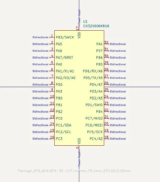
CH32V006K8U6 KiCad symbol

“Fully equipped” microcontroller with the bypass capacitor and the labels for all the GPIOs
Peripherals
At this point, the microcontroller is done in the sense that its power supply pins VDD and VSS are connected, and the GPIOs have their labels. The next step is to set up the peripherals such as the USB connector, the Crystal oscillator, the reset circuit and so on…
USB-C connector
First, let’s start with the USB connector. I use the “USB_C_Receptacle_USB2.0_16P” symbol for this purpose. The corresponding footprint I use is the “USB_C_Receptacle_GCT_USB4105-xx-A_16P_TopMnt_Horizontal”. This connector can be found by searching for the “USB4105-GF-A” manufacturing number, for example, on Mouser. Then, we work our way from the simpler to the more “complex” connections. GND obviously goes to ground. Then SBU1 and SBU2 are not connected (NC). Shield is connected to ground through a 1M resistor and a 4.7 nF capacitor in parallel. Although I might note here that I’ve been omitting the cap ever since, and I just use the resistor. I could be wrong, but I still keep the resistor, so it dissipates the charge, hopefully. The capacitor would help to further mitigate EMI issues, but this circuit is not an HF circuit anyway, so it is not that important.
Then, I connect the two D- pins and add a “D-” label, and then repeat the same, but with the D+ pins. Then CC1 and CC2 are each connected to the ground through a 5.1k resistor. The 5.1k resistors set the device to “default USB sink” mode, which then allows it to draw 500 mA from USB 2.0 or 900 mA from USB 3.0 connectors (at 5 V!). The resistors’ footprint is “R_0603_1608Metric”. They are both 0603 SMD resistors.
Then the VBUS first goes through a resettable fuse (“polyfuse”). This is a 6 V, 0.5 A PPTC resettable fuse, so it limits the maximum current on the VUSB line to 500 mA. Then the other side of the line is the +5 V line, so we assign the +5 V power rail to it. The footprint of the fuse is “Fuse_0805_2012Metric”.
Fun little side story: I’ve been buying Littelfuse’s “0805L050WR” resettable fuse because this is what popped up first when I was searching for PPTC fuses. They are super expensive; it costs $1.95/piece if I buy at least 10 pieces. When I compiled the BOM for this project, it really bothered me that the cost of this single component is almost as expensive as the rest of the other components together. So, I searched for another PPTC, and I was shocked. I discovered that this exact same type of resettable fuse exists from Yageo, but at a much lower price. It is $0.095/piece if I order at least 10 pieces. So, yeah, I could significantly reduce the cost of the board by exchanging this single component.
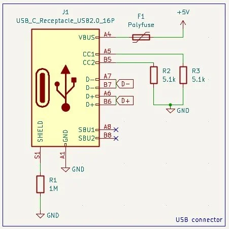
USB-C connector with the necessary resistors, a 500 mA fuse and some other connections.
Voltage regulator (5 V to 3.3 V)
Since we just established the 5 V rail, let’s continue with the voltage regulator. I will want the chip to operate at 3.3 V (even though it can run at 5 V, too). So, the circuit needs a voltage regulator that converts the 5 V down to 3.3 V. Since the voltage difference is not too large and we won’t run any high-current stuff through the regulator, we can use a low-dropout voltage regulator. The efficiency is not an issue here; we don’t need a DC-DC converter. I picked Texas Instruments’ LP5907MFX-3.3 250 mA low-noise, low quiescent current (12 uA!) regulator. If you want to save a little money and need more current on the 3.3 V line, you can pick the AP2112k-3.3TRG1 instead as a drop-in replacement. It can supply up to 600 mA current, but its quiescent current is 55 uA, which is maybe a bit too much compared to the other regulator if you are planning to design low-power devices.
Both regulators are super simple otherwise: Both their input and output pins should be equipped with a 1 uF electrolytic capacitor, and that’s all. Similar to the bypass capacitor at the microcontroller’s VDD pin, these capacitors are also 0603 capacitors. If we just duplicate the microcontroller’s bypass capacitor, we already have the footprint assigned, so it is an easy job. The output of the regulator is connected to the +3.3 V rail. Since we earlier already set the +3.3 V rail up for the microcontroller, we can just duplicate the symbol and add it to the output of the regulator.
Since we have power on our board now, let’s also indicate it. This indicator is just a 1k resistor and a red (or the colour of your choice) LED. The resistor can be duplicated from one of the earlier resistors, and we just need to change its value to 1k. The LED, however, needs a footprint assigned. I also chose 0603 size, so the footprint of the LED is “LED_0603_1608Metric“.

5 V → 3.3 V, 250 mA LDO

Simple LED power indicator fed from the 3.3 V rail.
Reset circuit
We hit up the datasheet again and go to the 3.3.10 NRST Pin Characteristics section and look at figure 3-5. According to the reference design, the reset circuit has an internal pull-up resistor. So, the purpose of the reset button is that it pulls the reset pin to ground when it is pressed. In parallel with the push button, there is a 100 nF capacitor to filter out jitter when the button is pressed and released.

Reset circuit according to the datasheet
I wanted to add a very tiny button here. Luckily, after some research, I finally found a tiny switch that I see on some other development boards and circuits. Luckily, it is very cheap ($0.19/piece if at least 10 pieces are ordered). It is the “PTS815SJM250SMTR LFS” tactile switch. If you search for this specific part in your KiCad library, you won’t find anything. So I will explain how to import symbols, footprints and 3d models from Mouser. It requires registration on Mouser, but it is worth it!
Once you find the product’s page, you will see a section just next to the product picture called ECAD model. If you click on the icon, a pop-up window will appear and it will show you all the necessary items: symbol, footprint and 3D model. Download the zip file, then open it. First, locate the folder called “3D”. This contains the step file of the 3D model. Unpack this file to your folder where you store the 3D models.
For me, this is the C:\Users\<username>\Documents\KiCad\9.0\3dmodels folder.
Then, locate the KiCad folder in the zip file. You’ll see a bunch of files, but in fact you only need the one that has the .kicad_sym and .kicad_mod extensions. Take the .kicad_sym file and unzip it into the folder where your keep the 3rd party footprints.
For me, this is the C:\Users\<username>\Documents\KiCad\9.0\footprints folder. If you don’t have a 3rd party footprint folder assigned in KiCad, then you also need to do that so the software can find these files. Go to the main project window and under “Preferences“, select the “Manage Footprint Libraries” item. In the form that pops up, under the “Global libraries” tab, click on the “+” icon at the bottom of the list, and enter a nickname, for example, “3rdParty” for the library. Then, in the next cell called “Library Path”, select the folder where you store the recently unzipped footprint file. Once it is done, click OK, and you are done with this part.
Finally, copy the .kicad_sym file under your symbols folder. This is the C:\Users\<username>\Documents\KiCad\9.0\symbols folder in my case. Then, again, go to the main project window and under “Preferences“, select the “Manage Symbol Libraries” item. In the form that pops up, under the “Global libraries” tab, click on the “+” icon at the bottom of the list, and in this case, enter the name of the part. I usually copy the part name from Mouser or enter a very descriptive name. Then, in the next cell, search for the .kicad_sym file you just added under your symbols folder. You can close this window by pressing OK.
Congratulations, you just learned how to import custom parts to KiCad in less than 5 minutes!
Now, we can return to the schematic editor and add the part to the circuit. We can see that the component has 4 pins. Two COM and two NO pins. These pins are wired internally, and when the switch is pressed, the pin pair 1-2 is connected to the pin pair 3-4. I wired it in a way that the NO_1 pin (pin 3) is directly connected to ground, and the COM_1 pin is connected to the reset pin on the microcontroller and also to the 100 nF capacitor. So, as the datasheet suggests, the reset pin is directly connected to the ground through this capacitor, and the direct connection is only realised when the button is pressed. Regarding pin 2 and 4, I just added a not-connected symbol to them since they can stay unconnected. The reset pin on the microcontroller is PA7. So, I added a label “NRST” to this pin and then duplicated it and added it to the switch as well.
Oscillator
The next step could be to add the external oscillator. According to the datasheet’s figure 3-4 a 24 MHz external crystal is connected to the XI and XO pins of the microcontroller, and the crystal is also connected with the appropriate load capacitance.
I wanted to go small, so I picked Kyocera AVX’s “CX2016FB24000B0FZZH1” 24 MHz crystal. It has a 2 mm x 1.6 mm outline, which is great! If we check the datasheet of the crystal, we see that it has 4 pins. Two of them are ground pins: pin 2 and pin 4. Pin 1 and pin 3 are the XI and XO pins. So, we can select the symbol called “Crystal_GND24” which is a generic symbol for crystals with GND connection on their pin 2 and 4. Or, we can download the symbol supplied by Mouser. Your choice. Immediately after adding the symbol to the circuit, we should assign a footprint. Again, you can use the one supplied by Mouser, or you can use the “Crystal_SMD_2016-4Pin_2.0x1.6mm” footprint. Then, we connect pin 2 and pin 4 to the ground directly and pin 1 and pin 3 via a capacitor. I added the XI label to pin 1 and the XO label to pin 3. Also, instead of 0603 capacitors, I selected 0402 (“C_0402_1005Metric”), because picoFarad capacitors are usually easier to find in this size. When we use a crystal, we need to add load capacitors to both XI and XO pins. The value of the capacitors is determined by 2 factors: the load capacitance of the crystal and the stray board capacitance. The first parameter is stated on the datasheet (6 pf), and the second is usually assumed to be around 4 pF. Then, plugging these numbers in the formula, we get 4 pF. So I have to use 4 pF capacitors.

One thing we must keep in mind is that since we use an external oscillator, we block PA1 (XI) and PA2 (XO) pins on the microcontroller. These pins are also ADC pins (ADC1 and ADC0 channels), so if you want to use all the ADC channels on the microcontroller, you might want to avoid using an external oscillator. Probably for very simple circuits, one can avoid the crystal, but an external crystal is good to have if a project relies on timing or uses USB, USART or similar peripherals. I would rather use an external crystal and then add an I2C or SPI ADC if I need more channels.

Crystal oscillator with its capacitors

Crystal oscillator according to the datasheet
USART-to-USB converter
So, the CH32V006K8U6 chip does not have any native USB; however, it has two USART ports. So, I compromised a bit on the GPIO pins, and I added a CH340N USART-to-USB converter chip to the circuit. This is not the fanciest converter chip, but I wanted to keep the budget tight, and I just wanted a simple USB communication between the microcontroller and the computer. The chip is included in the standard KiCad library, so we can just add it to the circuit.
Then, we need the datasheet of the CH340N chip. Since we use 3.3 V as the supply line, both V3 and VCC pins are connected to the +3.3 V rail, and then it is decoupled by a 100 nF capacitor. Then UD+ gets the duplicate of the D+ label we already made for the USB connector, and UD- gets the duplicate of the D- label. The GND pin is obvious. The RTS pin is not connected. Then the RXD pin is first connected to a 1k 0603 resistor, and the other pin of the resistor gets a label called USART-RX. This tells that this label belongs to the USB-to-USART chip’s RX pin. Similarly, we repeat the same pattern with the TX pin: a 1k 0603 resistor, and USART-TX label on the other pin.
Then, we take these labels and duplicate them. The USART-TX label goes to the USART1_RX (PD6) pin on the microcontroller, and the USART-RX label goes to the USART1_TX (PD5) pin on the microcontroller. It is very important that the wiring between the MCU and the converter chip is twisted. One chip’s RX is the other chip’s TX and vice versa. This is because what one chip Transmits, the other chip Receives. So, now we ensured that the board can be used as a USB COM device like an Arduino. The sacrifice we made here is that we blocked the PD5 and PD6 GPIO pins. So we lost 2 GPIOs, but especially, 2 additional ADC channels ADC5 and ADC6. If this is a problem, you can reassign the USART pins to other pins, or just use an external ADC.
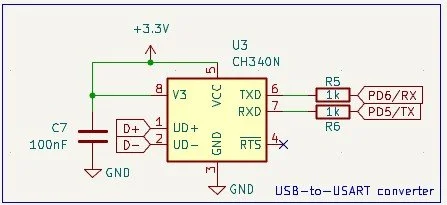
CH340N-based USB to USART circuit
SWDIO and GPIO
Now, two tasks remain. I put them under the same section because they are similar.
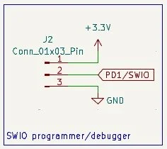
First, let’s talk about the SWIO. I created a similar connection that we can find on many similar boards: I used a 3-pin 2.54 mm header with the +3.3 V, SWDIO and GND pins on it. This is the programming/debugging port of the microcontroller. I simply added the power rails and the SWDIO label to this 3-pin connector (Symbol: “Conn_01x03_Pin“, Footprint: “PinHeader_1x03_P2.54mm_Vertical”).
Then, I added two 15-pin connectors (Symbol: “Conn_01x15_Pin “, Footprint: “PinHeader_1x15_P2.54mm_Vertical”) to the schematic. I mirrored one of them so I can nicely lay out the labels. The way I assigned the labels to each pin was a bit tricky. I had to see how my board should be laid out first and then I had to see how the traces would go to the respective connections. I finally decided to align the MCU so its pin 1 faces south and its pin 24 faces north. Then, I “split” the chip in two, or at least almost. Pins along pin 21 (PC7) and pin 5 (PA0) go on the left side of the board, and the rest of the pins go on the right side. We should remember that we have 5 pins (2x USART, 2x crystal, 1x reset) that are not connected externally.
So, for the left connector, I started with PC7 and went counter-clockwise towards PB4 on the microcontroller and added the applicable pins. On this side, I skipped PA7 since it is the reset pin, and I did not want to include it. So, there is one pin left empty and I added GND there. Although, if you want, you can add reset to pin 14 on the connector and then add PA0 to pin 15 instead of GND.
For the right connector, I added VUSB, +3.3 V and GND and the first three pins. Then I started from PC6 (the other side of the “split”) and went clockwise around the chip’s pins all the way until PD0. PA2 and PA1 are not added because they were “sacrificed” for he external crystal.

GPIO pin headers with labels and power rails
Programmer connector
PCB Layout
We finished with the schematics, and all the components have footprints assigned, so we can start working on the PCB layout. This process is (in my opinion) more of a form of art, but of course, there are some engineering rules we need to respect and follow. This board is fairly simple, so there are not too many rules we need to follow.
So, my goal was to make the board breadboard-compatible. So what I did is that I place the left side 15-pin connector in the centre of the area, and then I added a “dummy” 8-pin connector to the circuit. This part is not part of the circuit, but it helps with the alignment. So, when looking at the board, we have the USB-C connector, which is one of the limiting factors of the width of the board. So, I took a breadboard and figured that I could make the PCB narrow enough so that there are 2 rows that still remain empty on each side of the breadboard. That is exactly 8 pins wide.
Therefore, the currently placed 8-pin connector is a guide. I rotated it by 90° and placed it over the first pin of the left 15-pin connector. Then I placed the right 15-pin connector over the other end of the 8-pin connector, and after aligning everything, I deleted the 8-pin connector. I locked these 2 pins immediately, so I cannot mess up their position by accident while editing.
If you found this content useful, please consider joining my YouTube channel’s membership or leaving a donation.
Also, please consider using my affiliate links when buying relevant gadgets.
Dummy 8-pin connector to achieve the perfect spacing between the two 15-pin connectors quick&easy
Then, after selecting the edge cuts layer, I drew the board’s outline. I used the courtyard of the connectors as the guide. Then, a very important step, I added rounded corners to the board! I drew one, 1 mm radius arc and then duplicated it and created all four corners of the board. Then finally, I connected these corners and deleted the firstly laid out rectangle. I checked the board in the 3D viewer to see that everything looks correct so far. I want to emphasise that many YouTubers, even big ones, don’t even try to make the corners of their boards rounded, which I think is ugly, and it is also a poor design choice. Sharp edges often stay sharp and can cause injuries.
Once the board layout is complete, I draw a guideline along the centre of the PCB. This is to help centre the connectors and the microcontroller. I want these 3 items to be perfectly centered on the board. Then, since the board has 2 layers, I place a ground plane on the bottom layer. I flood the whole thing with ground.

Center guideline, rounded corners and copper fill
Then, before placing any components, under File/Board Setup/Design Rules/Constraints, I adjust a few things for the board. I set both the minimum clearance and track width to 0.15 mm. The minimum annular width and diameter are set to 0.1 mm and 0.5 mm, respectively. The copper to hole clearance is set to 0.15 mm, and the copper to edge clearance is set to 0.5 mm. The minimum through hole and the hole-to-hole clearance are both set to 0.2mm. The minimum thermal relief spoke count is set to 1. The other parameters I did not mention are left at their default values. Also, still in this window but under the Net Classes menu, we need to change the clearance and track width. The clearance must be 0.15 mm, and the track width must be 0.2 mm. Otherwise, we won’t be able to bring out the traces from the pins of the microcontroller.
Then I place the two leftover connectors on the PCB: at the top, I place the USB-C connector, and at the bottom, I place the 3-pin programming/debugging interface connector. Again, I check the 3D viewer to see if everything is aligned.
The from the USB connector I start to work my way through the board. It is an iterative process because the more components I put on the board, the more I have to change the other, already placed components.
First, I place the 1M resistor next to the USB connector and connect it to the shield. KiCad will complain that the other three pins should also be connected, but they are actually connected. The whole USB connector casing is a single piece of metal. So there is no need to connect the other three pins, because they are connected anyway. Then, I place the F1 fuse below the right side of the connector. Then I can place the two 5.1k resistors and the fuse as close as possible to the connector. Then, I can place the voltage regulator (2 capacitors + LDO) and the power indicator (LED + resistor) circuits.

Power section added to the board
Now, I can place the CH340N chip on the left side of the board, close to the USB connector, next to the LDO. Then I can place the two 1k resistors next to the TX and RX pins of the USART-to-USB chip, and I can also place its bypass capacitor.
Finally, I can squeeze the chip on the board. Remember, pin 24 points towards north (USB-C connector) and pin 1 points towards south (SWDIO connector). Then I fix the bypass capacitor for the chip and add the crystal with the two capacitors. One thing that we have to pay attention to is the fact that the chip must have a pin 0 as the pad underneath. So, we can double-click the pad and then assign a pad number (0) and net name (GND) to it. Then, finally, I add the reset button and its filtering capacitor.
I also added the three missing 3D models: the crystal, the CH340N’s SOIC-8 model and the push button’s model. I already had their step file in my 3D models KiCad library, but the parts had invalid paths defined for the files, so I had to fix them.
Now we have a rough layout for the board, and we see how the wires should go. Since the place available is quite crammed, we will need to use both sides of the board. First, I connect the components together because most of their pins will run on the top side of the PCB. Then I slightly readjusted them for better aesthetics and to be able to drag the wires more efficiently.

All parts, but no traces
Then, basically, I just work my way down from the top of the board. I start with the USB-C connector’s pins and then I gradually go towards the resistors, the fuse, the LDO and the voltage regulator and so on…
Then I proceed to the GPIO pins. Here, I need to be a bit more strategic because some pins can run on the top layer, but some of them will need to run on the bottom layer. This also affects the ground layer at the bottom because there will be quite a few wires that must run through the bottom layer. Either we accept that we get a somewhat chopped-up ground pour, or we change the stackup of the board and make it into a 4-layer board. This is a low-budget, low-performance board with nothing too fancy going on. No RF, no high-speed signals, nothing. So in my opinion, we can afford to chop up the bottom layer. Otherwise, we go back to the Board Setup, and under the Board Stackup/Physical Stackup, we change the board from 2 to 4 layers (copper layers = 4) and make the two inner layers the ground planes and the top and bottom are the signal and power layers. But I would not bother with this for this circuit. The only set of traces where we need a bit more attention is the D+ and D- traces between the USB connector and the USART-to-USB chip. I drew them as a differential pair, but I think this particular setup is not extremely picky about a proper impedance and so on. But let’s stay on the safe side.
Once all wires are in place, we can add text and labels to the pins. Again, this is more of an artistic process. We can, for example, totally omit the component IDs such as R1, U1, etc., and hide them. Technically, they do not need to be on the silkscreen because when it is assembled by a machine, the machine uses the fabrication data. The silkscreen is for human users. So, if you want, you can hide all the component IDs. Since I assemble the boards manually at home, I like to keep them because it helps to some extent.
One thing which is more important is to mark each pin on the two 15-pin connectors and on the 3-pin programming interface connector. I just follow the datasheet’s pin names, but without the “P” letter. So instead of writing PA0, I just write A0…etc. I also like to put my “make initials”, CS, on the board together with the year of design. I also put my website on the PCB, so people hopefully visit it more.
Finally, when everything is in place and the DRC is not throwing any more errors, I use mitxela’s KiCad plugin to make the traces curved. This is an optional step, but I really like the look of it, so I make the traces curved. Sometimes, some traces do not turn out to be nice or they cross forbidden areas…etc, so in that case, I erase the curved section of the trace, redraw it with a bit larger radius and apply the plugin again. A few small adjustments are usually enough.
When I am satisfied with the board, I export the Gerber files, compress them in a .zip package and place an order on PCBWay.com (affiliate link!).

KiCad render of the board
Get the PCB from PCBWay!