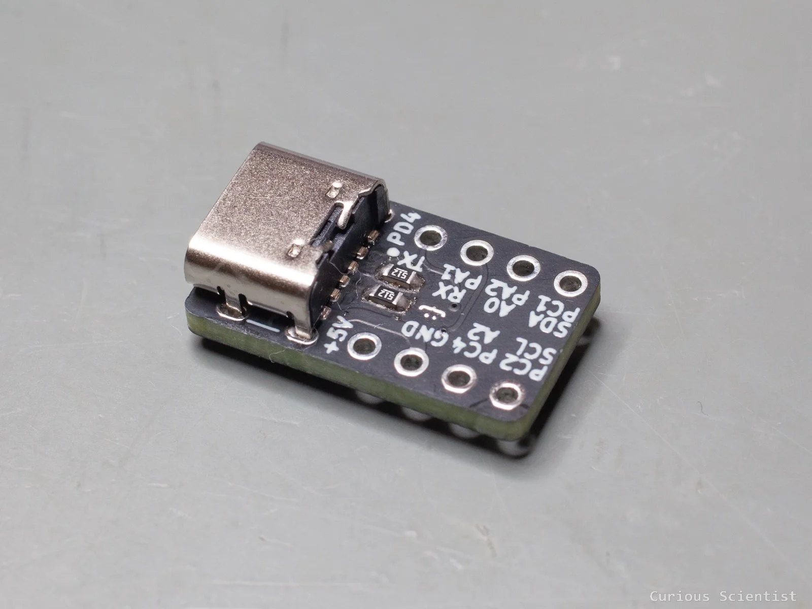
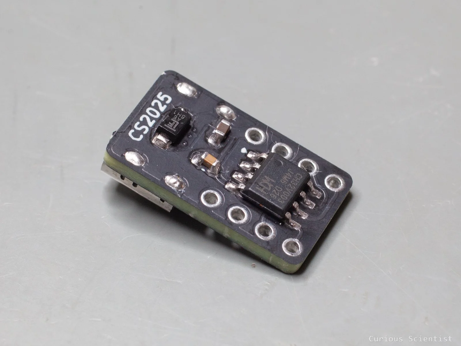
A tiny microcontroller board based on the CH32V003J4M6 chip
In this article, I show you how and why I designed this cute little board. I wanted something small but relatively capable, and since I have some experience with the CH32V003J4M6 chip from my other projects (remote-controlled fume extractor, breadboard voltmeter, low-power applications), I decided to make this board based on the chip. This chip has an SOIC-8 package, so it is a simple 8-pin SMD chip. Similar to the Attiny85, but it is a bit more powerful.
Introduction
I think I don’t need to introduce this chip too much because I have talked about it enough in my other articles and videos (remote-controlled fume extractor, breadboard voltmeter, low-power applications), plus it has a datasheet that can be read by the curious readers.
However, I can tell more about the motivation of the project. Recently, I made a few circuits that control something simple, so it does not require a lot of GPIO pins and powerful computation capacity. Some of these projects were based on this chip, while others were based on Attiny85 chips. The thing is that while the Attiny85 is around $1.5 per piece, I can buy 10 pieces of the CH32 chip for the same price. It is a considerable difference when it comes to scaling up numbers. Since the CH32 has everything that the Attiny85 has, except SPI, which I don’t need anyway, I decided to design a board based on this chip. (Although, later I will show that, in fact, SPI would have been nice in a specific case.)
The chip is stupid simple. It works “bare-bone”, and since I am planning to use it with 5 V logic devices, I don’t even need a voltage regulator. The chip will only receive a 100 nF decoupling capacitor on its power pin, but otherwise it will run off the 5 V of the VUSB line.
Circuit design
As I hinted, the circuit design is very simple, mainly because of the chip’s simplicity.
I also went with the following design choices to preserve simplicity:
5 V-only operation (no 3.3V-compatibility)
USB-C connector and should withstand currents up to 3 A
No need for USB/USART communication through the USB port → Simpler, 6-pin USB-C connector
No need for the reset button
Miniature footprint
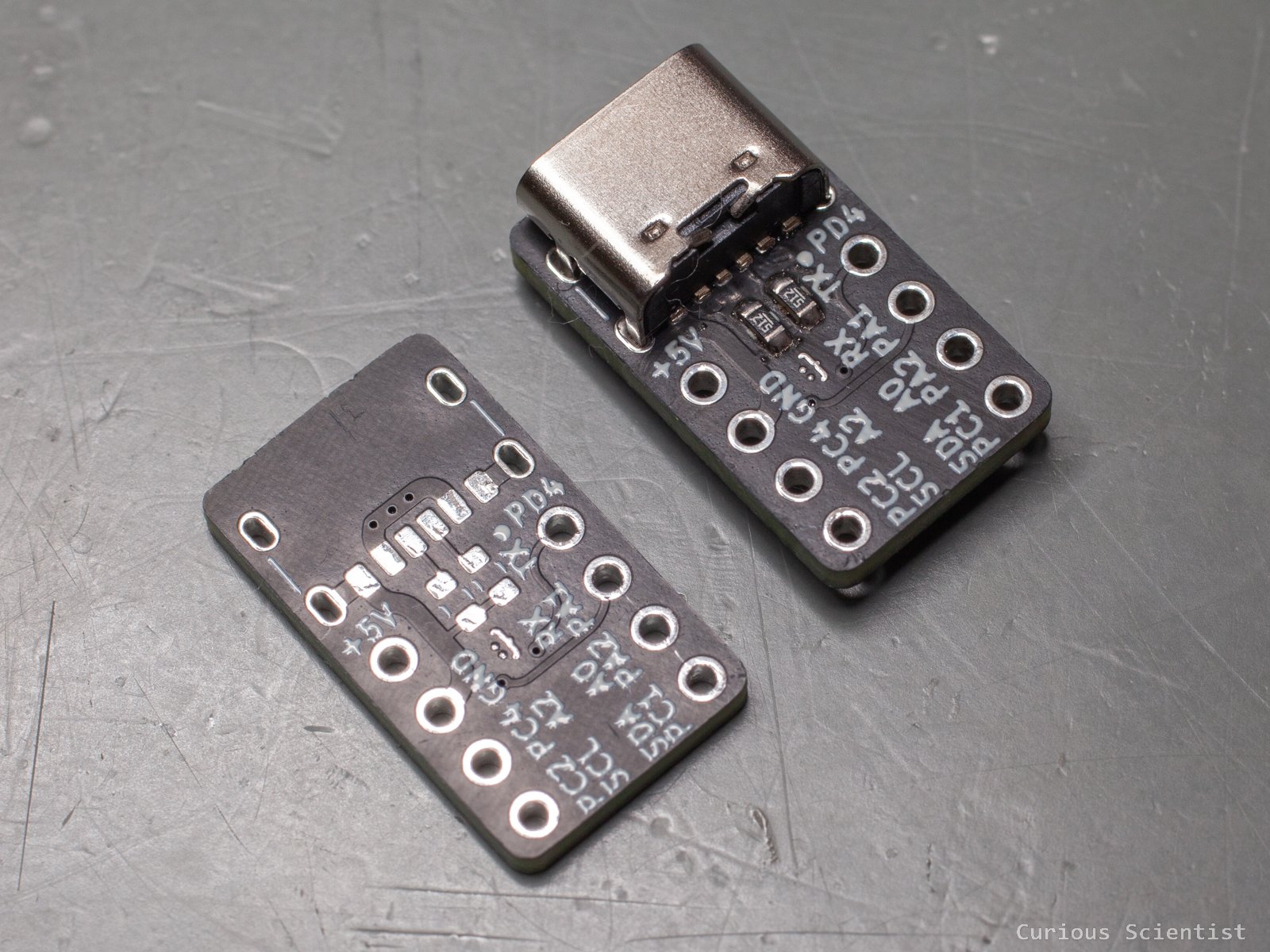
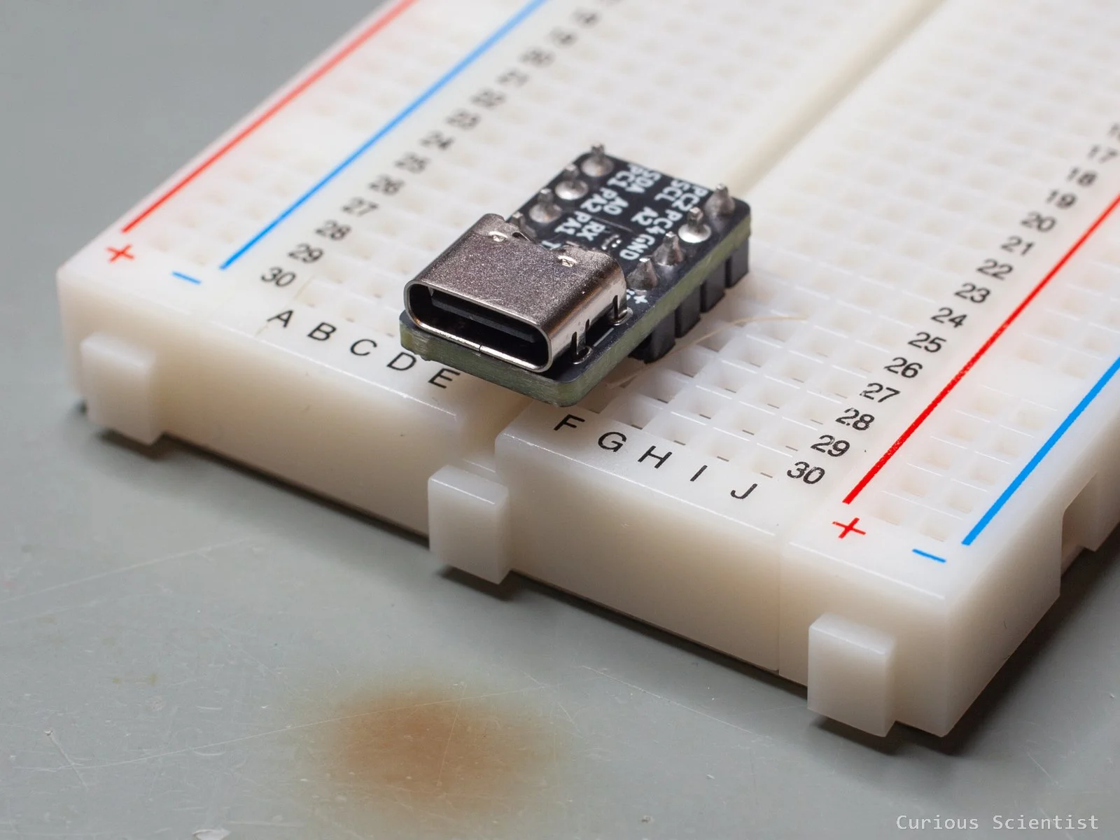
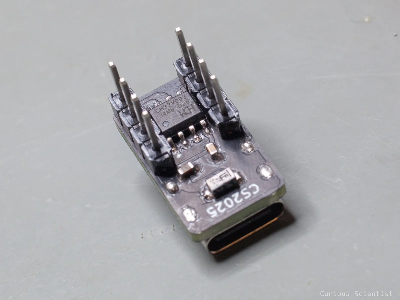
In fact, the miniature footprint here is taken seriously. The circuit board is not much wider than the USB-C port itself. It is a perfect coincidence that the 2.54 mm header pins can be lined up perfectly so that they don’t exceed the width of the USB-C port, and I can plug the board into a breadboard. The distance between the two header pins is exactly 4 pins, which is the same distance as the distance between the adjacent pin rows at the centre of a breadboard.
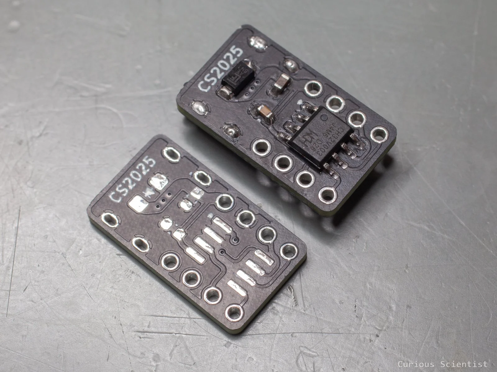
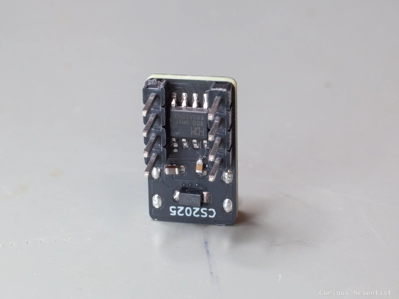
Another great coincidence is that if I rotate the chip, it fits between the two rows of 2.54 mm headers just fine. I had to juggle with the wiring a bit, and I needed a few vias, but I managed to arrange everything neatly. However, this required the board to be 2-sided. Both the bottom and the top of the board contain components. Luckily, there are very few components, and they are large enough to be soldered by hand. One can use a hot plate for the bottom layer and then finish up the top with a hot air tool or even with a soldering iron. It depends on patience and dexterity.
In total, the board has 7 components: 2 capacitors, 2 resistors, 1 microcontroller, 1 TVS diode and 1 USB-C port. I do not count the two 4-pin headers, because they are not mandatory for the circuit. Especially, if the board is built into some project, it can be omitted.
Some use cases
Below, I share a few cool use cases to justify the board design.
1. NeoPixel (WS2812B) LED controller
This one is a simple but cool use-case, in my opinion. One WS2812B LED can take up to 60 mA, so in theory, ~50 LEDs could shine at max brightness with white colour. The LEDs only need a data line and a 5 V power supply, and both can be provided by my board. When the device is powered with a proper USB-C adapter (Ikea Sjöss 45 W), it is possible to draw up to 3 A on the 5 V line.
2. OLED thermometer/hygrometer based on the BME-280 chip.
With a stylish 3D-printed case, this device can be a nice addition to your home. Both the OLED display and the BME-280 modules are I2C devices, so they require the same two pins (SDA and SCL) apart from the power pins. This device requires very little energy, so even a simpler adapter like the Ikea Småhagel can be used.
3. Real-time clock based on the DS3231 module
Again, with a stylish 3D-printed case, this device can be a cool little gadget in your home. The module can communicate with the device via I2C. With a carefully chosen display and stylish fonts, it can be a cool accessory. The device is not power-hungry, so a simple USB adapter is enough.
In the rest of the article, I will focus on the first use case, and I will explain how my timer and DMA-based library works.
Timer (and DMA)-based driver for the WS2812B LEDs
So, I am going to ride the wave of my previous video here and show an alternative way of driving these RGB LEDs. Previously, I used a smart hack implemented on the SPI bus, and here, I will use a timer. The main reason why I use a timer here is that this microcontroller does not have an SPI peripheral. So, the next obvious choice is using a timer.
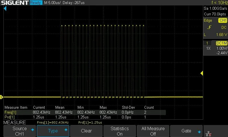
To reiterate, the LED works with an 800 kHz timing basis. The bits that are passed to the LED in the 24-bit package are set by pulses. They are described as “Code 0” and “Code 1” pulses. The total period of a pulse is 1250 ns (1/800 kHz), and basically, we need to change the duty cycle of the pulse to generate Code 0 and Code 1.
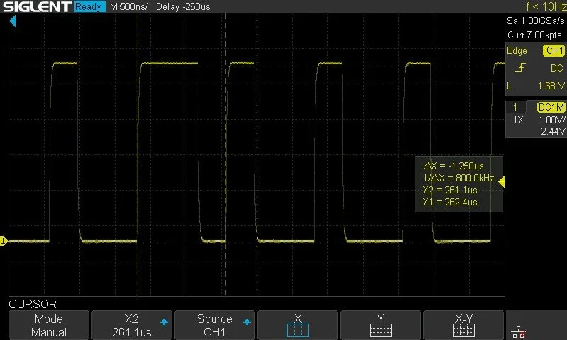
Code 0 is high for 400 ns and low for the rest (850 ns). Code 1 is high for 850 ns and low for the rest (400 ns).
If we look at how timers work, we can see that we don’t even need to bother about calculating the duty cycle and such. A timer is mainly configured by setting its ARR (auto-reload register) and CCR (capture compare register) values. ARR tells the timer when to reset counting, and CCR tells the timer when to flip the sign of the output signal. At least this is a very simplified picture of it.
So, by considering the CPU’s ticks, which is 20.83 ns in the case of a 48 MHz microcontroller, we can see that the 1250 ns wide pulse needs 60 ticks. Then, the 400 ns is 19 ticks and the 850 ns is 41 ticks. So, we can set the timer’s ARR (60) and CCR (19 or 41) accordingly. The only thing that we need to remember is that the code adds “+1” to these numbers under the hood, so when I say 60, it is “60-1”. It is one of those gotcha things that can bite you...
So, now we know these pulses very well. We understand how to generate an 800 kHz square wave with 50% duty cycle, so we can see the timing of the LED. And then we can further configure the CCR value to generate the Code 0 and Code 1 pulses. But, the big question is: how to alternate the CCR values in subsequent pulses? When we send a data package to an LED, we need to send out 24 of these Code 0 and Code 1 pulses. And they won’t be all 1s or 0s. Therefore, we must find a way to dynamically generate and manipulate the subsequent pulses. Possibly, without putting any burden on the CPU.

Well, here comes the DMA (Direct Memory Access) to save the day!
For each LED, we need to transmit one 24-bit slot, which contains 24, 1250 ns long slots (pulses), and for each slot, the CCR is either 19 (Code 0) or 41 (Code 1). So, whenever there is a timer update (a slot is finished), the DMA should load the next CCR value to the timer’s CCR register from a pre-built buffer. These values are stored in a buffer when the colour-to-bit conversion is done, before actually instructing the LED to shine with some colour. Once the transfer is done, we just keep the line low for at least 50 us (Treset), and we are good to go.
So, we need to set up the timer and the DMA accordingly. The timer is rather straightforward. I picked the PC4 pin on the microcontroller because it does not have any other peripheral that I might need later. It has timer one, channel 4 (TIM1CH4) available, so we will work with that. Since I built the code into a library, I made most of the parameters adjustable by modifying the macros’ values at the top of the library file. The timer does not need any special attention, and I already have a tutorial on timers where I defined the timer basically the same way. The only differences are the following:
I use TIM1CH4, so the output compare (OC) part must be described on channel 4. Therefore, for example, we initialise the clock by TIM_OC4Init() instead of TIM_OC1Init().
I disable both TIM_OC4PreloadConfig() and TIM_CtrlPWMOutputs(). They’ll be enabled later when we actually generate the pulses.
The DMA is a bit more special. I touched DMA in my ADC-related tutorial, but here we do a bit more. So, first, let me repeat that the way we generate the pulses is that when the timer generates an update event, the DMA should load the next CCR value to the timer’s CCR register. Why is this important? Because we need to map the peripheral (TIM1) to the correct DMA channel based on the event.
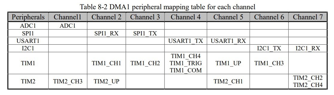
As the image above shows, the update event (TIM1_UP) is under channel 5. So the DMA must be initialised with channel 5. Another good thing to know is the peripheral address of the timer. Again, we have timer 1, channel 4, so the peripheral address is TIM_CH4CVR. And, since we work with a peripheral now, the transfer direction is “memory to peripheral” (DMA_DIR_PeripheralDST).
The rest of the parameters are straightforward and typical (default) parameters. The peripheral address does not need increments, so it is disabled. We always read the same timer channel. On the other hand, the memory address should be incremented, so in each iteration, the next item of the buffer is accessed. This is important because this buffer stores the next CCR value that should be loaded in the timer.
And just as a reminder, the data size here is 32 bits for a word and 16 bits for half word. This is easy to mess up because older architectures might refer to words as 16-bit units.
static void ws_timer_init(void)
{
    GPIO_InitTypeDef GPIO_InitStructure = {0};
    TIM_OCInitTypeDef TIM_OCInitStructure = {0};
    TIM_TimeBaseInitTypeDef TIM_TimeBaseInitStructure = {0};

    RCC_APB2PeriphClockCmd(RCC_APB2Periph_TIM1 | RCC_APB2Periph_GPIOC);

    GPIO_InitStructure.GPIO_Pin   = GPIO_Pin_4;
    GPIO_InitStructure.GPIO_Mode  = GPIO_Mode_AF_PP;
    GPIO_InitStructure.GPIO_Speed = GPIO_Speed_30MHz;
    GPIO_Init(GPIOC, &GPIO_InitStructure);

    TIM_Cmd(TIM1, DISABLE);

    TIM_TimeBaseInitStructure.TIM_Period        = 60-1;
    TIM_TimeBaseInitStructure.TIM_Prescaler     = 0;
    TIM_TimeBaseInitStructure.TIM_ClockDivision = TIM_CKD_DIV1;
    TIM_TimeBaseInitStructure.TIM_CounterMode   = TIM_CounterMode_Up;
    TIM_TimeBaseInit(TIM1, &TIM_TimeBaseInitStructure );

    TIM_OCInitStructure.TIM_OCMode      = TIM_OCMode_PWM1;
    TIM_OCInitStructure.TIM_OutputState = TIM_OutputState_Enable;
    TIM_OCInitStructure.TIM_Pulse       = 19;
    TIM_OCInitStructure.TIM_OCPolarity  = TIM_OCPolarity_High;
    TIM_OC4Init(TIM1, &TIM_OCInitStructure );

    TIM_OC4PreloadConfig(TIM1, TIM_OCPreload_Disable);
    TIM_ARRPreloadConfig(TIM1, ENABLE);

    TIM_CtrlPWMOutputs(TIM1, DISABLE);
}
static void ws_dma_init(uint16_t *buf, uint16_t len)
{
    DMA_InitTypeDef DMA_InitStructure = {0};

    RCC_AHBPeriphClockCmd(RCC_AHBPeriph_DMA1, ENABLE);

    DMA_DeInit(DMA1_Channel5);

    DMA_InitStructure.DMA_PeripheralBaseAddr = (uint32_t)&WS_TIM->CH4CVR;
    DMA_InitStructure.DMA_MemoryBaseAddr     = (uint32_t)buf;
    DMA_InitStructure.DMA_DIR                = DMA_DIR_PeripheralDST;
    DMA_InitStructure.DMA_BufferSize         = len;
    DMA_InitStructure.DMA_PeripheralInc      = DMA_PeripheralInc_Disable;
    DMA_InitStructure.DMA_MemoryInc          = DMA_MemoryInc_Enable;
    DMA_InitStructure.DMA_PeripheralDataSize =     DMA_PeripheralDataSize_HalfWord;
    DMA_InitStructure.DMA_MemoryDataSize     =     DMA_MemoryDataSize_HalfWord;
    DMA_InitStructure.DMA_Mode               = DMA_Mode_Normal;
    DMA_InitStructure.DMA_Priority           = DMA_Priority_VeryHigh;
    DMA_InitStructure.DMA_M2M                = DMA_M2M_Disable;

    DMA_Init(DMA1_Channel5, &DMA_InitStructure);
}
To push out a 24-bit sequence of pulses that encodes the colour and intensity of an LED, we need to start and stop the timer and DMA in a specific way.
First, we apply a reset latching which holds the line LOW for more than 50 us. This ensures that the subsequent pulse train does not get contaminated with garbage pulses, and the LED will interpret the pulse train as it should be interpreted. I used 80 us for my SPI-based implementation, so I used the same here. Apart from latching the PC4 pin for 80 us, I also disabled the timer (TIM1) and its outputs.
Also, it is important to remember that there’s a difference between using the PC4 pin as a GPIO pin or as an output pin for TIM1CH4. When it is used as a GPIO pin, its mode should be set to GPIO_Mode_Out_PP, which sets the pin as a regular push-pull GPIO pin. When we want to use the same pin with its timer-related functionality, we need to redefine the mode as GPIO_Mode_AF_PP. This uses the pin’s alternative function (AF), which is the timer output pin.
static void ws_reset_latch(void)
{
    GPIO_InitTypeDef GPIO_InitStructure = {0};

    TIM_Cmd(TIM1, DISABLE);
    TIM_CtrlPWMOutputs(TIM1, DISABLE);

    GPIO_InitStructure.GPIO_Pin   = GPIO_Pin_4;
    GPIO_InitStructure.GPIO_Speed = GPIO_Speed_30MHz;
    GPIO_InitStructure.GPIO_Mode  = GPIO_Mode_Out_PP;
    GPIO_Init(GPIOC, &GPIO_InitStructure);
    GPIO_ResetBits(GPIOC, GPIO_Pin_4);

    Delay_Us(80);

    GPIO_InitStructure.GPIO_Mode = GPIO_Mode_AF_PP;
    GPIO_Init(GPIOC, &GPIO_InitStructure);
}
Then comes the fun part. Now we just focus on one LED, but my code is generalised for N LEDs. N depends on the hardware, especially the amount of RAM. To make sure that the timer and DMA start from a clear state, I disable everything timer and DMA-related and clear the relevant flags.
Then, I re-initialise the DMA according to the previously discussed parameters, addresses, etc.
The next step is to sync the timer, so I set its counter to zero and clear its flag. Then, I enable the DMA requests on timer update and start the DMA. Then I generate an update event on the timer and clear the flag so the first real PWM bit that is pushed to the LED starts cleanly. After this cleanup, the main output of the timer and the timer itself are enabled. This will also start triggering the DMA since now the timer will start generating update events. The code waits until the transfer complete flag changes. After the flag is changed, the timer and DMA are stopped, and another reset latching is performed to finally clean things up.
So, in theory, this would work very nicely. However, in practice, it does not.
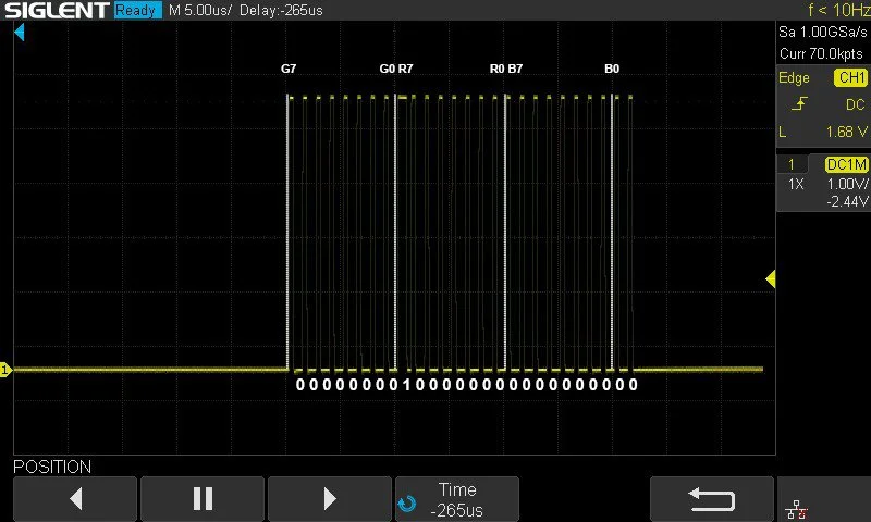
When I, for example, send out an instruction that should set the first LED to red colour at half brightness (128) while the global brightness is set to 255, so that I really should get half brightness, I get a very dim green colour on the first LED.
By looking at the pulses, I can see 24 pulses, so that should be OK at first glance. However, when I take a closer look at the pulses, I see a glitch. I can see that, yes, the LED physically should be dim green because, according to the pulses, the bits of the green colour are 00000001, and the rest of the bits for the other colours are 0. So the whole pulse is 0000 0001 0000 0000 0000 0000. This is wrong. And if you think a little and recall how the colours are packed in the 24-bit package, you will quickly see that the pulses are shifted. That single “1” should be one position to the right. Or, we can think about it as if a pulse were missing from the beginning. With an extra pulse at the beginning, the binary would be 0000 0000 1000 0000 0000 0000, which would lead to a correct colour.

25 pulses with an extra inserted pulse at the beginning. This results in a correct pulse sequence interpretation by the RGB LED, but still has issues.
Actually, this only solves half of the issues.
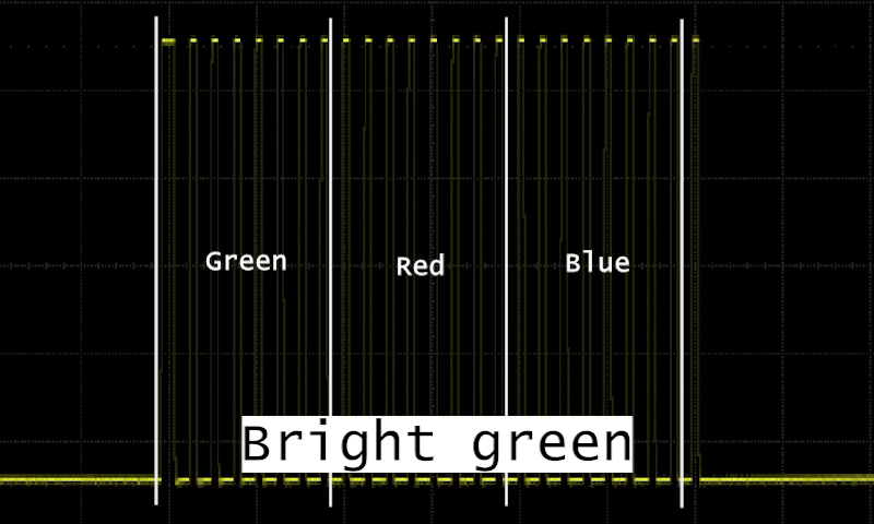
Now, let’s do the following exercise. Let’s toggle the very last bit of the pulse train. This essentially means that we blink the LED’s B0 bit by setting it to 0 and 1 with some delay in between. The LED should show a blinking, dim blue colour. Instead, we see a blinking bright green LED with occasional blue hints. Why?
So, the end of the pulse train is still wonky, and this can cause the last bit to “spillover” to the next pulse train and become its first bit. This would be then 0000 0000 0000 0000 0000 0001 (dim blue) and 1000 0000 0000 0000 0000 0000 (bright green). The first bit of the pulse train is G7, and if that bit is set to 1, which translates to 128 in decimal, it will set the green LED to half brightness. Well, guess what the blinking LEDs' colour is!?
To make this funnier, we can make the problem disappear by setting the number of LEDs (LED_COUNT) to two or anything larger than one. We still toggle the first LED as before, but now the first LED’s pulse train is followed by an extra pulse (the starting pulse of the 2nd LED). Now the first LED blinks dim blue, and since we haven’t assigned anything to the 2nd LED, it does not care about the pulse, plus the bits are zero anyway.
So, this suggests to us that we also need to add a “closing pulse” when we build the CCR buffer to make things work with a single LED. After adding the closing pulse, we get a dim, blinking blue LED. The last bit does not spill over to the next pulse anymore.
A correct pulse sequence that gets interpreted correctly by the RGB LED and it is invulnerable to spillover-issues.
static void ws_send_ccr_slots(uint16_t *buf, uint16_t slotCount)
{
    ws_reset_latch();

    TIM_Cmd(TIM1, DISABLE);
    TIM_CtrlPWMOutputs(TIM1, DISABLE);
    TIM_DMACmd(TIM1, TIM_DMA_Update, DISABLE);

    DMA_Cmd(DMA1_Channel5, DISABLE);
    DMA_DeInit(DMA1_Channel5);

    DMA_ClearFlag(DMA1_FLAG_GL5);
    DMA_ClearFlag(DMA1_FLAG_TC5);

    ws_dma_init(buf, slotCount);

    TIM_SetCounter(TIM1, 0);
    TIM_ClearFlag(TIM1, TIM_FLAG_Update);

    TIM_DMACmd(TIM1, TIM_DMA_Update, ENABLE);

    DMA_Cmd(DMA1_Channel5, ENABLE);

    TIM_GenerateEvent(TIM1, TIM_EventSource_Update);

    TIM_ClearFlag(TIM1, TIM_FLAG_Update);

    TIM_CtrlPWMOutputs(TIM1, ENABLE);
    TIM_Cmd(TIM1, ENABLE);

    while (DMA_GetFlagStatus(DMA1_FLAG_TC5) == RESET) { }

    TIM_ClearFlag(TIM1, TIM_FLAG_Update);
    while (TIM_GetFlagStatus(TIM1, TIM_FLAG_Update) == RESET) { }

    TIM_Cmd(TIM1, DISABLE);
    TIM_CtrlPWMOutputs(TIM1, DISABLE);
    TIM_DMACmd(TIM1, TIM_DMA_Update, DISABLE);

    DMA_Cmd(DMA1_Channel5, DISABLE);

    ws_reset_latch();
}
Pulse spillover glitch.
static uint16_t ws_build_ccr_from_strip(const ws2812b_t *strip)
{
    uint16_t idx = 0;
    ccrBuf[idx++] = 19;

    for (uint16_t led = 0; led < strip->count; led++)
    {
        uint8_t g = strip->pixels[led].g;
        uint8_t r = strip->pixels[led].r;
        uint8_t b = strip->pixels[led].b;

        if (strip->brightness != 255)
        {
            uint16_t br = strip->brightness;
            g = (uint8_t)((g * br + 127) / 255);
            r = (uint8_t)((r * br + 127) / 255);
            b = (uint8_t)((b * br + 127) / 255);
        }

        for (int bit = 7; bit >= 0; bit--) ccrBuf[idx++] =
        bit_to_ccr(g & (1 << bit));
        for (int bit = 7; bit >= 0; bit--) ccrBuf[idx++] =
        bit_to_ccr(r & (1 << bit));
        for (int bit = 7; bit >= 0; bit--) ccrBuf[idx++] =
        bit_to_ccr(b & (1 << bit));
    }

    ccrBuf[idx++] = 19;
    return idx;
}
Some final thoughts about this approach. It is a neat approach, but if the microcontroller supports SPI, I’d choose SPI instead of the TIM+DMA approach. This CH32V003J4M6 was only able to drive 34 LEDs with my demo code. I tested the same code with my CH32V006K8U6 development board, and due to the 4x more RAM (8k instead of 2k), I was able to run roughly 4x more LEDs. I tested it with my 16 x 16 array, and I could compile the code and light up roughly half of the LEDs. Then, I switched to SPI on the K8U6 and all of a sudden, the size of the code and RAM usage dropped, and I could drive all 256 LEDs.
Buy the products via my affiliate links:
Get the full code from my GitHub!
Get the board from PCBWay!