CH32V003F4P6 with WS2812B RGB LEDs
In this video, I continue my CH32 tutorial series, and I show you another hardware-specific library that I developed. This time, it is a library that can drive the WS2812B RGB LEDs. These LEDs are also known as “NeoPixel” LEDs, and they are very popular in various Arduino projects. Nowadays, these LEDs are extremely cheap. One can buy 50 pieces for less than $3. But then, one has to spend another $3 to get a microcontroller that can drive them. So, why not use a microcontroller that is almost as cheap as one LED?! Hence, I introduce this project that helps you to drive many of these LEDs with a very cheap (but powerful enough) microcontroller. Plus, I will use a neat approach to drive the LED with somewhat outside-of-the-box-thinking.
Introduction: the WS2812B RGB LED
So, this is a very popular RGB LED that can be found in different LED modules, and sometimes, even development boards have it embedded. It is a small 5 mm x 5 mm device, so it is not too difficult to find a place for it in your board if needed. I even covered the basic principles of this LED in one of my Shorts on YouTube. But basically, the package contains a small processor and three LEDS with the basic red, green and blue colours. The LED’s onboard chip decides how to drive these three LEDs based on the 24-bit data package that it receives via its data IN pin.
The LED has 4 pins: A power supply pin, a ground pin, a data IN pin and a data OUT pin. The typical operating voltage of the LED is around 3.5 V - 5.3 V, so the best is to run it with a 5 V power supply. It does not work with 3.3 V logic. It is important to notice that an LED at full brightness and white colour (all three onboard LEDs are fully on) draws around 60 mA. So, even when it is driven from the 5 V rail of a microcontroller (and NOT a GPIO pin!), only a dozen or so LEDs can be driven simultaneously. And with the power draw, heat is generated, too, which one must be aware of.
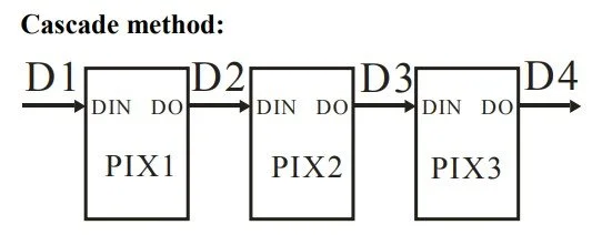
The data IN pin is also 5 V-rated, so it should be used with a 5 V microcontroller, or a level shifter must be used. If multiple LEDs are chained, then the first LED’s data OUT pin goes to the second LED’s data IN pin, and then the second LED’s data OUT pin goes to the third LED’s data IN pin… and so on… The LEDs must be connected in series. In my demonstration, I use a small strip that has 8 LEDs connected in series.
Working principles
The driving of the LED is relatively easy. The LED expects a 24-bit data package that consists of three 8-bit packages; each byte for one colour. Each colour, red, green and blue has its own byte, and the value of the byte determines the brightness of the given colour. So, each colour can be controlled with a number between 0-255, where 0 means that the corresponding LED is OFF, and 255 means that the LED is at full brightness.
The bits in the above-mentioned 24-bit data package are set according to the sequence chart, which is available in the datasheet of the LED. Each bit is a sequence of high and low pulses with a relatively strict timing. To set a bit 0, its pulse should be high (T0H) for 400 ns, and then it should be low (T0L) for 850 ns. To set a bit 1, its pulse sequence should look the opposite: the high time (T1H) should be 850 ns, and the low time (T1L) should be 400 ns. All these timings allow a +/- 150 ns deviation.
To send a reset (RET) signal, the data IN line should be kept LOW for more than 50 microseconds. This indicates the end of the data stream after all the LEDs’ data is sent out. It can also be used before starting the data transmission to flush out any partial data.
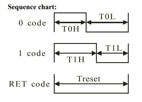
Pulse-sequences to produce “0 code”, “1 code” and “RET”.
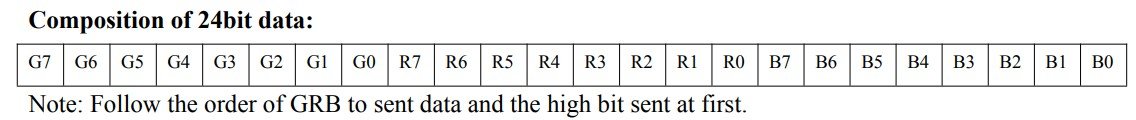
As we can see above, the 24-bit data, read from left to right, starts with the green colour's high bit and then ends with the blue colour's low bit. So, it is important to see that the colour order is GRB and not RGB. But this is completely OK, we just have to pay attention when we write the code. Each LED has such a 24-bit package. Each bit between G7-B0 is assigned with 0 or 1 by applying one of the above-mentioned pulse sequences called “0 code” or “1 code”.
SPI implementation
After thinking a little bit, I figured that this protocol could be implemented with the help of SPI. SPI has the speed we need, and it can push out bytes with very strict timing. Just what we need. I have already made an introductory video and article on the SPI communication, so I won’t repeat the whole thing there. I will just reiterate a few lines.
So, the good thing about the SPI is that it works with well-defined clock pulses and for each pulse, it pushes out a bit on the MOSI line (or reads one on the MISO). Therefore, if we find a good prescaler value for the SPI clock, we can create building blocks that represent the “0 code” and the “1 code” I showed earlier. And then these packets can be sent out via the MOSI line to the data IN pin of the LED, and the LED will interpret the packages as pulses kept LOW or HIGH for a certain time.
When it comes to the clocks, let me just repeat that we need a pulse with 400 (+/- 150) ns width and a pulse with a 850 (+/- 150 ) ns width. The clock speed of the SPI is the clock speed of the microcontroller, which, in my case, is 48 MHz. I found the prescaler 16 to be a good value. This brings the SPI speed down to 48 MHz / 16 = 3 MHz, so each pulse period is 333.3 ns long. I could have used a smaller prescaler for a better resolution, but soon I will explain why I haven’t done it. So, I used this 333.3 ns as the building block for the 0 and 1 codes.
Code 0 thus consists of one 1 and three 0s (“1000”). And Code 1 consists of three 1s and one 0 (“1110”). These are simply the bit values in a byte that are being pushed out via the MOSI pin to the data IN pin of the LED. Since the timing of the SPI bus determines the width of a bit, this trick can be used to generate relatively well-timed pulses with custom pulse shapes. When we need the pulse to be HIGH, we set the corresponding bit to 1, and when we need the pulse to be LOW, we set the corresponding bit to 0.
The reason why I haven’t picked a smaller prescaler, for example, 4, is the following. In the case of a prescaler 4, the SPI clock would be 12 MHz. This is an 83.3 ns period. So, we could reproduce a 400 ns wide HIGH pulse more accurately by setting 5 MOSI bits HIGH. This would result in a 416.5 ns wide HIGH pulse, which is much closer to 400 ns than 333.3 ns. But now we need many more bits to describe a pulse, which eats more RAM. If we needed to construct the 850 ns pulse, we would need 10 bits to be set to LOW. Actually, 9 would still be enough (749.7 ns) because it is still within the tolerance (+/- 150 ns). So, in total, instead of 4 bits to create Code 0 and 1, we need 4x more, 16 bits. Of course, this is trivial because we increased the resolution by 4-times, but I wanted to demonstrate it and explain it carefully.
Timing requirements for Code 0 and Code 1.
SPI clock (top) and MOSI signal (bottom). The highlighted MOSI represents a “1” (HIGH) pulse, which is 333.3 ns wide
SPI clock (top) and MOSI signal (bottom). The highlighted MOSI represents a “0” (LOW) pulse, which is 1000 ns wide.
Code 0 and Code 1 sequences. Code 0 consists of a 333.3 ns wide HIGH and a 1000 ns wide LOW pulse and it is coded as “1000” on the MOSI line. Code 1 consists of a 1000 ns wide HIGH and a 333.3 ns wide LOW pulse, and it is coded as “1110” on the MOSI line.
Coding
Now we know the practical stuff, so let’s discuss the most important parts of the code.
Let’s begin with the SPI initialisation. In fact, it is very close to the code I used for the SPI demonstration, but there are some key differences.
For example, I only defined PC6 (MOSI) as a GPIO. Since we don’t need the rest of the pins (CS, MISO, SCLK) physically, we don’t need to define them and initialise them. So, as you can see, only MOSI is defined. After initialising it, I set it to LOW, so it does not do anything weird.
Furthermore, I won’t need bidirectional SPI communication because I just use the SPI to send out data; therefore, the SPI_Direction is defined as SPI_Direction_1Line_Tx.
The clock polarity and phase are set so they generate consistent pulses; however, they can most likely be anything because we do not use the SCLK line. We only want the MOSI to be clocked out precisely, but it does not matter if it is clocked out at the rising or falling edge of the clock pulse…etc.
Then, the most important line is the SPI_BaudRatePrescaler that determines the final SPI clock speed. As I demonstrated in my little back-of-the-envelope calculation, the clock should be set to 3 MHz, which is achieved by prescaling the 48 MHz CPU clock by 16. Thus, we set the prescaler to be SPI_BaudRatePrescaler_16.
Then, there are only a few other parameters I initialised with the default values, and that’s that. The final step is to enable the SPI.
Once again, I would like to emphasise that we don’t use the SPI for data-based communication. The bits we send to the WS2812B LEDs do not represent any intelligible data. They don’t go to registers in a sense, as they go when we use, for example, the ADXL345 accelerometer. We just utilise the tight timing of the bits of the SPI protocol and generate pulse sequences. And this is why we can set most of the SPI parameters to their default values without punishment.
Then, the other function I want to discuss is the function that encodes the GRB colours to SPI-MOSI bits. We use GRB instead of RGB within the code and functions because that’s how the WS2812B chip expects the data.
So, the function expects a parameter which is a pointer pointing to the LED strip object. This object stores the number of LEDs (count), the RGB fields (colours) and the brightness values.
So, the outermost for() loop iterates through all the LEDs in the strip. First, we grab the green, red and blue colour values taken from the pixels fields of the struct. Then we check if the brightness is lower than maximum. If it is lower, then we do a scaling based on the global brightness value (br) we defined and stored in the strip struct. As I mentioned, each colours are represented by its brightness in the RGB LED and the mixture of the brightnesses of the red, green and blue LEDs will make up the final colour emitted by the RGB LED. But this final colour can be very bright, or very faint as well. This is what we control with this scaling.
Then, since the WS2812B expects the bits in G, R and B order, we arrange the bytes accordingly into an array.
Then, we encode the bytes into MOSI patterns. The next inner for() loop iterates through all three colour channels (v) and packs the colours into SPI bytes. At the end, we will create three times four bytes packed into the spiBuf[] array.
The bi starts at 0 and goes until bi < 3, so the for loop iterates three times. At each iteration, we pass the bi-th bytes[] item to the variable v, which represents a colour channel. Let’s say v = 1010 0101.
The innermost for() loop extracts and encodes the WS bits. Each v is an 8-bit value that describes the brightness of a selected colour. In the first iteration of bi (bi = 0), this is the G7-G0 bits of the green colour. The bit starts at 0 and goes until bit < 8, and it is incremented by 2 for each iteration, which means that in total, there will be 4 iterations in this for loop. We have 8 bits per colour, and each iteration produces two bits.
The variable b1 is determined by performing a logical AND operation between v and 0x80 (or 0b1000 0000). Since v was selected to be 1010 0101, the result will be 1 (true), so b1 = CODE1, or 1110.
Then, we shift the v to the left by one, so the new v is v = 0100 1010. We do a logical AND operation again, which will return 0 (false), so b2 becomes CODE0, or 1000.
Then, we combine these two nibbles into an 8-bit number. The b1 becomes the upper nibble, so we shift it up inside the 8-bit integer, and b2 is simply masked to be the lower nibble. So this gives spiBuf[0] = 11101000. These nibbles are G7 and G6. We need to repeat this process three more times to get the G5-G4, G3-G2, and G1-G0 pairs.
Then, the middle for loop advances to bi = 1, and we repeat a similar procedure to obtain the values for R7-R0. And then after another bi++, we obtain B7-B0.
At the end, the spiBuf[] will be passed to another function that simply pushes out the assembled nibbles to the MOSI line. This will create the necessary pulse patterns to drive the LED.
static void InitializeSPI1(void)
{
    GPIO_InitTypeDef GPIO_InitStructure = {0};
    SPI_InitTypeDef  SPI_InitStructure = {0};

    RCC_APB2PeriphClockCmd(RCC_APB2Periph_GPIOC | RCC_APB2Periph_SPI1, ENABLE);

    GPIO_InitStructure.GPIO_Pin = GPIO_Pin_6;
    GPIO_InitStructure.GPIO_Mode = GPIO_Mode_AF_PP;
    GPIO_InitStructure.GPIO_Speed = GPIO_Speed_50MHz;

    GPIO_Init(GPIOC, &GPIO_InitStructure);

    GPIO_ResetBits(GPIOC, GPIO_Pin_6);

    SPI_I2S_DeInit(SPI1);

    SPI_InitStructure.SPI_Direction = SPI_Direction_1Line_Tx;
    SPI_InitStructure.SPI_Mode = SPI_Mode_Master;
    SPI_InitStructure.SPI_DataSize = SPI_DataSize_8b;
    SPI_InitStructure.SPI_CPOL = SPI_CPOL_Low;
    SPI_InitStructure.SPI_CPHA = SPI_CPHA_1Edge;
    SPI_InitStructure.SPI_NSS = SPI_NSS_Soft;
    SPI_InitStructure.SPI_BaudRatePrescaler = SPI_BaudRatePrescaler_16;
    SPI_InitStructure.SPI_FirstBit = SPI_FirstBit_MSB;
    SPI_InitStructure.SPI_CRCPolynomial = 7;
    SPI_Init(SPI1, &SPI_InitStructure);

    SPI_Cmd(SPI1, ENABLE);
}
static uint16_t encode_grb_to_spi(const ws2812b_t *strip)
{
    uint32_t out = 0;

    for (uint16_t i = 0; i < strip->count; i++)
    {
        uint8_t g = strip->pixels[i].g;
        uint8_t r = strip->pixels[i].r;
        uint8_t b = strip->pixels[i].b;

        if (strip->brightness != 255)
        {
            uint16_t br = strip->brightness;
            g = (uint8_t)((g * br + 127) / 255);
            r = (uint8_t)((r * br + 127) / 255);
            b = (uint8_t)((b * br + 127) / 255);
        }

        uint8_t bytes[3] = { g, r, b };

        for (int bi = 0; bi < 3; bi++)
        {
            uint8_t v = bytes[bi];

            for (int bit = 0; bit < 8; bit += 2)
            {
                uint8_t b1 = (v & 0x80) ? CODE1 : CODE0;
                v <<= 1;

                uint8_t b2 = (v & 0x80) ? CODE1 : CODE0;
                v <<= 1;

                spiBuf[out++] = (uint8_t)((b1 << 4) | (b2 & 0x0F));
            }
        }
    }
    return (uint16_t)out;
}
Buy the products via my affiliate links:
Get the full code from my GitHub!