TCD1304 Linear CCD - Driving the CCD
In this video I will show you step-by-step how you can program the STM32F401CCU6 microcontroller using STM32CubeIDE to drive the TCD1304 linear CCD. My source code is capable of driving the CCD using the electronic shutter function and it is capable of sending the raw data to the computer via USB. The code allows you to change the shutter speed which allows you to read the CCD in any kind of lightning conditions.
You can find the datasheet of the TCD1304 CCD here.
Introduction to the CCD
First, I want to talk about CCDs in general, so you can understand how they work and why do we program it in a way we do.
CCD stands for Charge-Coupled Device. It is a piece of semiconductor that can capture light, transform it into electrons and electronic signal. Each pixel is basically a capacitor that holds charge which is proportional to the amount of incident light. The photoactive layer which is located on the top of the CCD captures the light and converts it into electric charge. Each capacitor (pixel) will hold a charge proportional to the light it was exposed to. If the shift gate (SH) is clocked often (short integration time), the accumulated charge will be small, therefore the image might appear darker. If the toggling of the shift gate is slower (long integration time), the image might appear brighter or even over-exposured. Once the exposure is done, the content of the capacitors is being shifted out step-by-step. The stepping is done by the shift register. Once the pixels are shifted out the reset gate is triggered (integration clear gate - ICG) which clears away the potentially accumulated charge so we can capture the light again into empty potential wells.

Extremely oversimplified drawing of a CCD. The gate electrodes are used to shift the charge between the different potential wells.
Timing requirements for driving the CCD
As it we can see it on the image to the right, the CCD is controlled by three signals:
SH - Shift gate clock
ICG - Integration clear gate clock
ϕM - Master clock (shift register clock)
As a response to these signals, the CCD outputs a signal on its OS pin. The signal consists of 3694 elements. D0-D31 elements are dummy pixels, S1-S3648 are the actual 3648 pixels which is the real signal, and D32-D45 are also dummy pixels.
The above information tells us that we need to generate 3 different clock signals (SH, ICG and ϕM), and we need to capture one signal (OS).

Clock characteristics of the master clock and data rate.
Based on the clock characteristics of the TCD1304, the typical value of ϕM is 2 MHz and at this value, the data rate is 0.5 MHz or 500 kHz. So, now we also know that ϕM should be 2 MHz and the data rate of the ADC that captures the output voltage of the OS pin should be 500 kHz. This means that the signal that triggers the ADC should be as rapid as 500 kHz. Thus, there will be 4 signals needed to be generated in total: the already mentioned 3 clock signals (SH, ICG and ϕM) for driving the CCD, and another clock for triggering the ADC of our microcontroller in order to correctly read the output voltage of the CCD.

Timing requirements of the TCD1304 linear CCD using the electronic shutter function

Timing requirements for the three driving signals ICG, SH and ϕM.
Reading further into the datasheet we can see more information about the necessary timings for the driving signals (image to the left). The most crucial part is the careful timing between the SH and ICG signal.
After ICG goes low, SH should go high within 1 us (t2) and should stay high for at least 1 us (t3).
After SH goes low, ICG should go low within typically 5 us (t1).
The rising edge of ICG at t4 should be aligned with the falling edge of ϕM typically within 20 ns.
Below we can also see how the ICG and SH are aligned when we use the electronic shutter function. The readout starts when the ICG goes low and it lasts until it goes low again. The integration time is determined by the period of the SH signal.
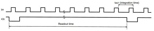
Pulse timing of ICG and SH for using the electronic shutter function.
Doing the mathematics
Before I jump into the coding part, I would like to share all the formulas that I am going to use for the coding, so you can have a general understanding of how these numbers are obtained.
First of all, we will work with square waves, more precisely PWM (Pulse Width Modulation) signals with different duty cycles. The simplest starting point is the correlation between the ADC frequency and the number of pixels that we need to shift out because these two numbers will determine the readout time which will determine the frequency of the ICG signal.
The ADC frequency is 500 kHz. Based on f = 1/t → t = 1/500 kHz = 2 us. This means that 1 pixel is fitted into a 2 us time slot. Based on the timing requirements we have 3694 pixels to read, therefore the total readout time is 3694 x 2 us = 7388 us. This is about 135.4 Hz. This also determines the upper limit of the integration time which is also 7388 us since in the most extreme scenario we only have 2 SH pulses: one after the start of the readout time and one after the finish of the readout time.
Luckily, the frequency and the duty cycle of the ICG, ϕM and the ADC trigger is constant, we only need to calculate and configure their parameters once.
On the other hand SH is a bit more complicated. We would like to generate different PWM signals between 10 us integration time and 7388 us integration time. From now on, for the sake of simplicity, I round 7388 us up to 7500 us. As we will see it later, it is totally fine to do so.
To nicely align the signals of SH and ICG it is important to select the frequency and duty cycle carefully. I made a list of integration times and I calculated the frequencies and the duty cycles, so later on it will be easier to apply these numbers to calculate the values of the registers for the timers to generate the proper PWM signals.
| t_int (us) | F (Hz) | Duty cycle (%) |
|---|---|---|
| 7500 | 133.3 | 0.053 |
| 2500 | 400 | 0.16 |
| 1250 | 800 | 0.320 |
| 500 | 2000 | 0.8 |
| 100 | 10000 | 4 |
| 75 | 13333.3 | 5.333 |
| 50 | 20000 | 8 |
| 20 | 50000 | 20 |
| 10 | 100000 | 40 |
Starting from the ICG, we want to know the frequency and duty cycle. As I said, I use 7500 us as the ICG → ICG readout time. Based on this time, the frequency is 133.3 Hz. We also know it from the timing requirements of the ICG signal, that the width of the PWM pulse consists of t1+t2+t3 times. Based on the typical values, this is 5000 ns + 500 ns + 1000 ns, so at least it is 6500 ns. For the sake of simplicity. I let it to be exactly 10000 ns or 10 us because this is also the minimum integration time. So, if we have a signal that is 7500 us long and the on time is 10 us, we can calculate the duty cycle which is 10 us / 7500 us = 0.13333%.
ICG characteristics: 133.3333 Hz and 0.13% duty cycle.
The characteristics of the SH signal is a bit more complicated because it is not only the frequency, but also the duty cycle is changing. I chose the pulse width of SH to be constant 4 us at all frequencies (integration times). Therefore the duty cycle can always be recalculated by knowing the frequency (period) and the on time of the pulse which is always 4 us. For example, at 10 us integration time, we see that the total pulse width is 10 us, and the on time of the pulse is 4 us, therefore, the (4 us / 10 us) * 100 = 40% (the x100 multiplier comes in to express the value in %).
I calculated some typical values for the SH signal and show them in the table to the right. Later below I will show you how to convert these numbers into the correct register values for the STM32 microcontroller.
As we set up 7500 us for the ICG → ICG time, it is a good idea to only use an integer fraction of it for the integration time so this way the signals will match nicely (e.g. don’t use 4976 us as integration time).
Programming the STM32F401CCux using the STM32CubeIDE
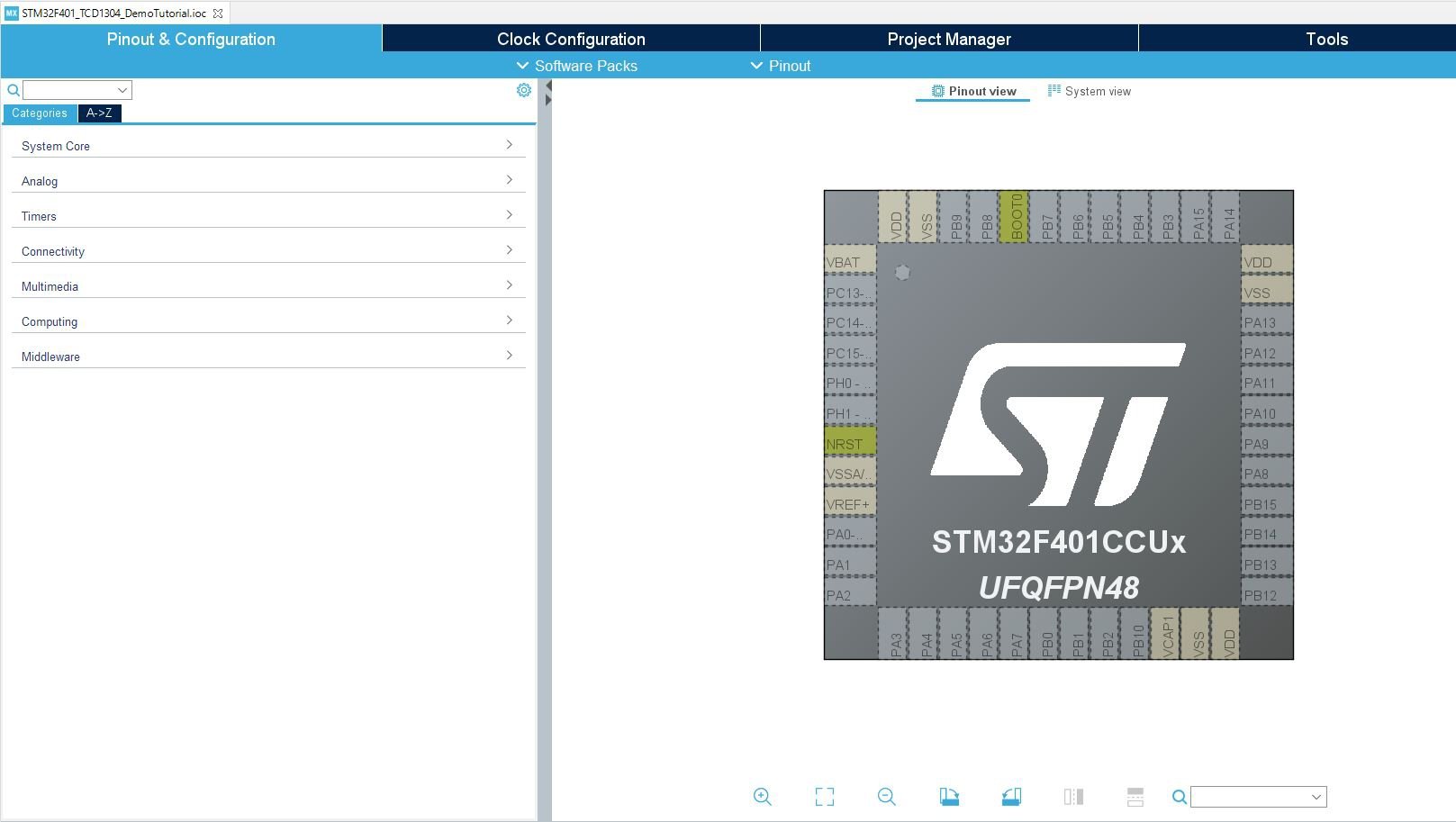
This part will be meticulously explained because there are no good resources on the internet about the programming part. I am using the STM32CubeIDE with the HAL API. Once again, the selected MCU is an STM32F401CCU6.
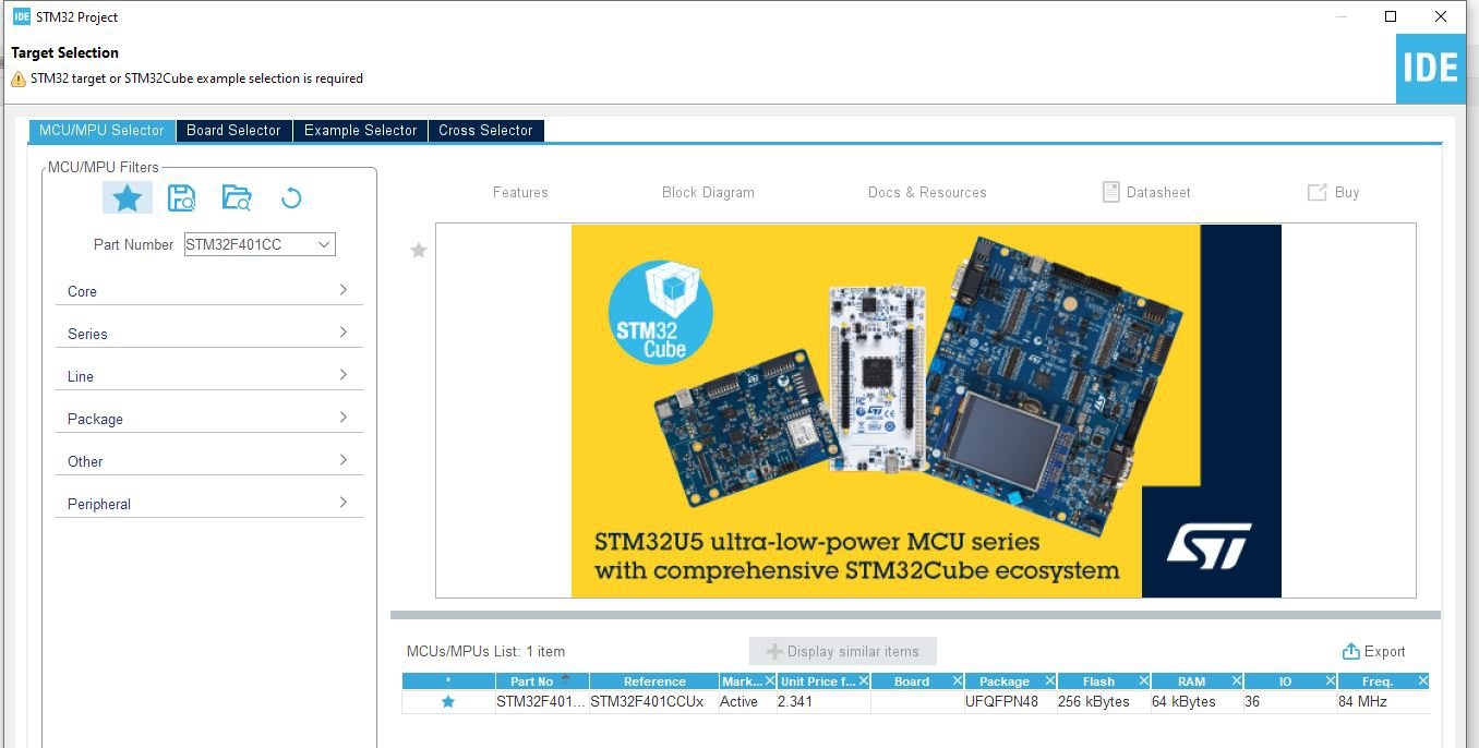
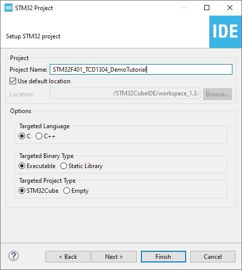
Let’s first create a new STM32 project. After clicking, the target selector comes up. Type STM32F401CC to the part number and select the microcontroller from the items. Click next, then give some name to your project and click finish. After this you should end up at the main screen which shows the peripherals on the left side and the chip on the right side.
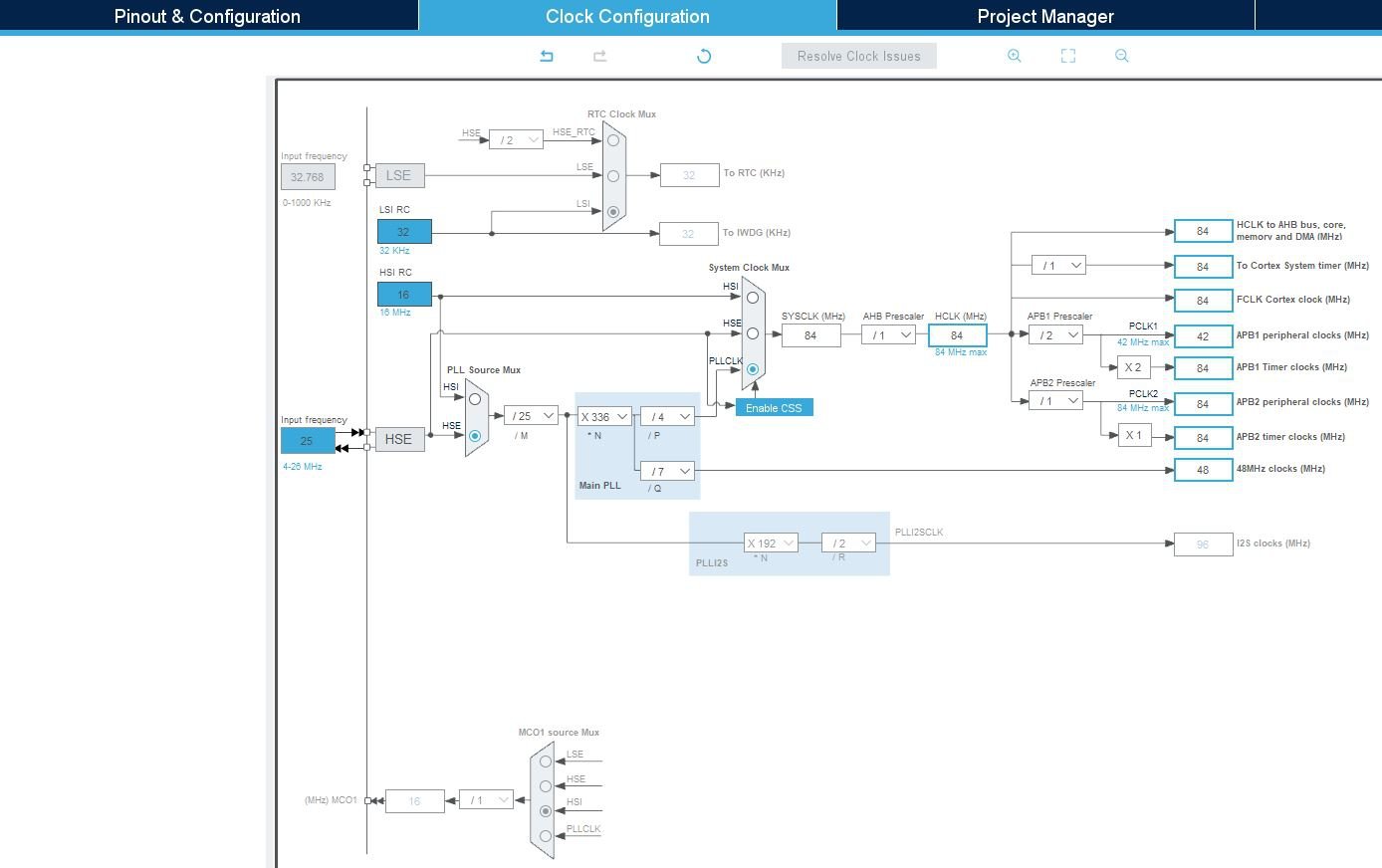
First two things we should fix is the USB communication and the clock configuration. We need to take care of the USB first because it need the the High Speed Clock (HSE) which will influence the available clock frequencies. Since we want to use the clock frequencies in further calculations it is a good idea to fix these values from the very beginning.
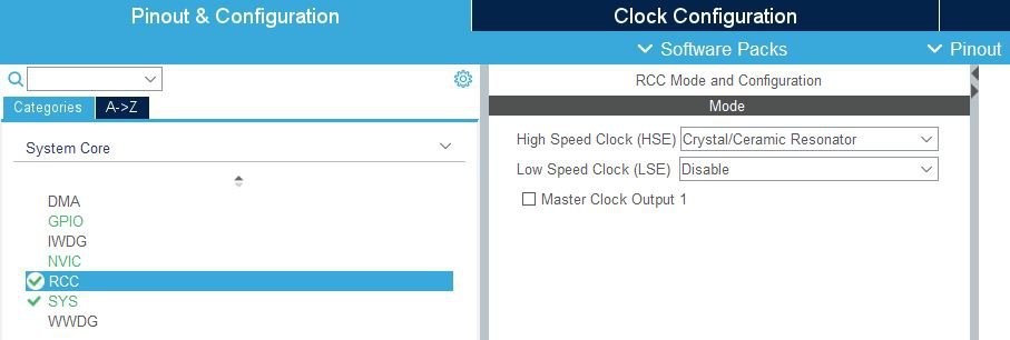
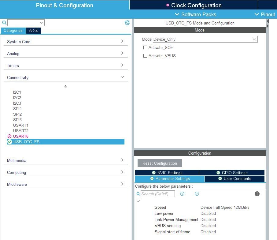
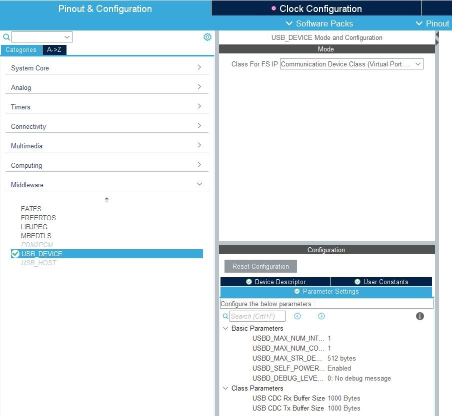
Go to System Core, select RCC, then under the RCC Mode and Configuration, select Crystal/Ceramic Resonator for the HSE. Next, go to Connectivity, select USB_OTG_FS and select Device_Only mode. Finally, go to Middleware, select USB_DEVICE, then select Communication Device Class (Virtual Port).
After this, go to Clock Configuration and enter 84 MHz to the HCLK field and press enter. The software will tell you that it needs to recalculate the clock configuration. Approve it, and let the software work. Make sure that you get the exact same values as I have. It is crucial to have the proper clock values. Since we know the main clock frequency, we can calculate the time of 1 clock cycle which is 1/(84 MHz) = 11.9047619 ns. This will be useful later. Also, make sure that you use a lot of digits when you calculate these periods and frequencies, otherwise you might end up having slightly misaligned signals or strange values.
Timers, the most crucial peripherals for this project
Now we deal the timers. Here let’s first talk about the timers and their resolution. The MCU I picked has four general purpose timers: TIM2, TIM3, TIM4 and TIM5. TIM3 and TIM4 are 16-bit timers, TIM2 and TIM5 are 32-bit timers. This is very nice because the 32-bit timers allow us to have really long integration times. But in fact, if we stick to the 7500 us maximum integration time, we can solve everything by using the prescaler for the timers. I will show both options so you can use the popular STM32F103C8T6 a.k.a. “blue pill” for driving this CCD. However, I will discuss everything for my MCU, the STM32F401CCU6.
Let’s assume that we want to utilize the 32-bit timers. Therefore, the SH and ICH signals will be generated by the 32-bit timers, the ϕM and the ADC trigger signals will be generated by the 16-bit timers.
Before doing anything in the software, let’s understand very quickly how the timers work and how they generate the PWM signal. The timer is basically a counter. The counter counts up (or down) once for every clock pulse. A 16-bit timer can count up to 2^16 -1 = 65535, and a 32-bit timer can count up to 2^32 - 1 = 4294967295 before overflowing. To generate a PWM signal we need to know the main clock frequency of the MCU which is 84 MHz in this case. Earlier we calculated that the period of this frequency is about 11.9 ns. Also, we need to know the parameters of the PWM signal: the period and the duty cycle. As an example from one of the parameters for the SH, let’s say that we want a signal whose period is 10 us and whose duty cycle is 40%. Now we have to translate these numbers to the “language of registers”. There are two registers, the auto reload register (ARR) and the capture compare register (CCR) which are used to generate the PWM signal. Basically, CCR says how long the PWM on the output should stay high from the starting of the counter (CNT) and ARR says how long the timer should count from the starting of the counter.
With numbers: if we want a 10 us long, 40% duty cycle signal using a 11.9 ns (84 MHz) period clock, the signal should be high for 4 us. CCR = 4 us / 11.9 ns = 336, and ARR = 10 us/ 11.9 ns = 840.
In this example I assign the timers in the following way:
TIM2: ICG, TIM3: ϕM, TIM4: ADC trigger, TIM5: SH.

Typical illustration of the PWM signal generated by the timer. The counter starts from zero and the PWM signal starts as high. It stays high until the counter reaches the value of the CCR. At this point, the PWM signal goes low and stays low until the ARR value where the counter is reset and starts over from zero.
TIM3
Let’s start first the two most simple timers: TIM3 and TIM4 because they do not need any special attention.
First, I set up TIM3 for ϕM. Go to Timers, check the checkbox called Internal Clock, select Channel 1 as "PWM Generation CH1” from the drop down list. Then below in the configuration, fill in the following values. As we know, we need 2 MHz for the master clock. 2 MHz is 84 MHz / 42. So, we set the counter period (ARR) to 42-1. The “-1” part comes in because the program always adds one to the entered number in the background (I guess, to avoid division with zero) so in order to get exactly 42, we enter 42-1, so we also indicate that 1 was subtracted. Since we want a 50% duty cycle, the Pulse (CCR) should be half of ARR: CCR = 21-1. As a result we have this nice square wave with the exact parameters that we want to have.

Master clock signal (ϕM) as it is seen by an oscilloscope.

9. Configuration page of the master clock (ϕM) signal.
TIM4
Next stop is the ADC trigger. As we decided earlier based on the datasheet of the TCD1304, the frequency is 500 kHz, or 0.5 MHz. This makes the math easier because 1/4th the frequency of ϕM means that we need to count four times longer. With numbers it means that the ARR register will be (42x4)-1 = 168-1. In this case, I picked the duty cycle to be 25% which means that the CCR register will be (ARR/4)-1 = 42-1. We go to TIM4, Mode and Configuration, select the Internal Clock by checking its check box, then select Channel 4 as “PWM Generation No Output” because we only need this signal “internally”. We use Channel 4, because this channel will be used as the trigger for the ADC.

ADC trigger signal as it is seen by an oscilloscope.
(Note: There is no output coming from the ADC trigger, but for the sake of demonstration I put the signal on the output)

10. Configuration page of the ADC trigger signal.
TIM2 and TIM5
Now we only have ICG and SH left. This topic is a bit more difficult because ICG should trigger SH and there should also be a slight delay between ICG and SH after ICG goes low. Also, as I am using the basic circuit which is shown in the datasheet of the TCD1304, therefore we have to change the polarity of one of the PWM signals.
Since TIM2 triggers TIM5 via ITR0 (see Table 54 in the RM0368 reference manual), we first set up TIM2 as the master as well as the timer for ICG. Earlier we calculated the frequency (133.333 Hz) based on the 7500 us readout time. 133.3 Hz (133.333333…. Hz) gives exactly 630000 for the ARR value. And here we immediately see the need of the 32-bit timer if we do not want to use the prescaler. With a prescaler of 10, we get 63000 for ARR which is OK for a 16-bit timer as well (STM32F103C8T6!). I stick with the 32-bit timer. We also calculated the necessary duty cycle earlier: 0.133333% → 0.00133333 * 630000 = 840. So, ARR = 630000-1 and CCR = 840-1. As usual, we select the Clock Source as Internal Clock, and we select Channel 1 as “PWM Generation CH1”. In the configuration, ARR and CRR are set to the above calculated values, and we also enable the Master/Slave Mode (MSM bit), and we set the Trigger Event Selection to Enable (CNT_EN). This means that the triggered timer (TIM5) will be triggered when the counter of the TIM2 timer is enabled.
Now let’s look at TIM5 which is the timer for SH. From my experiments I know that we need a rather fast integration time if we want to use the CCD exposed to normal light conditions. I saw some people putting a black electrical tape over the CCD, but it is completely unnecessary. If you can control the integration time properly, you do not need to struggle with the tape. So, let’s choose 20 us as the integration time. Keep in mind that the SH’s duty cycle is dynamic, it is a function of the integration time. In fact, the CCR register’s value will be always the same, whatever the integration time is, but if you want to express the duty cycle in percentage, it will be always different. At 20 us, the duty cycle is 20% which is ARR = 1680-1 and CCR = 336-1. In the configuration panel, we first select Trigger Mode under Slave Mode, then we set the Trigger Source as ITR0. Then, we check the Internal Clock checkbox, and we select Channel 3 as “PWM Generation CH3”. It is Channel 3 and not Channel 1 because once we select the ADC, Channel 4 becomes unavailable. In the configuration, we fill in ARR and CCR, then in the Trigger Output Parameters, we set the MSM bit to Enable and the Trigger Event Selection should be Reset. Finally, the CH polarity should be low.

11. TIM2 timer configuration for the ICG signal. Polarity is set to high but if you use the HEX inverter, it becomes low which is the same alignment as in the datasheet.

12. TIM5 timer configuration for the SH signal. Polarity is set to low but if you use the HEX inverter, it becomes high which is the same alignment as in the datasheet.
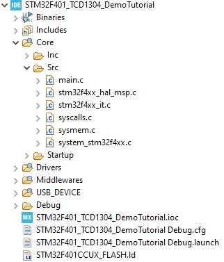
After setting up everything, press the save button to generate the code for the timers and everything else. Then, in the project tree, navigate to Core/Src and open the main.c.
Go to main.c and navigate to the /* USER CODE BEGIN 2 */ part and insert the following code there:
HAL_TIM_PWM_Start(&htim3, TIM_CHANNEL_1); //PA6 - fM
HAL_TIM_PWM_Start(&htim4, TIM_CHANNEL_4); //ADC
HAL_TIM_PWM_Start(&htim2, TIM_CHANNEL_1); //PA0 - ICG
HAL_TIM_PWM_Start(&htim5, TIM_CHANNEL_3); //PA2 - SH
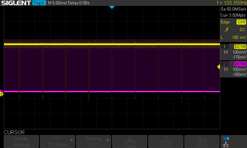
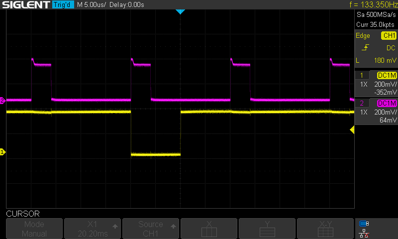
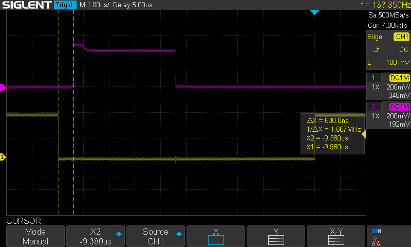
This code will start all the timers needed to drive the CCD. But! the code is not yet perfect at this point because as you can see (see the 3rd image to the right in the gallery), there is no delay between SH and ICG. In order to add the delay we need to insert an additional line which will give an initial value for the CNT register of the TIM2 timer and which will cause a 600 ns difference between the ICG and SH.
HAL_TIM_PWM_Start(&htim3, TIM_CHANNEL_1); //PA6 - fM
HAL_TIM_PWM_Start(&htim4, TIM_CHANNEL_4); //ADC
HAL_TIM_PWM_Start(&htim2, TIM_CHANNEL_1); //PA0 - ICG
__HAL_TIM_SET_COUNTER(&htim2, 66); //600 ns delay
HAL_TIM_PWM_Start(&htim5, TIM_CHANNEL_3); //PA2 - SH
NOTICE: Please notice that for these three images to the right, I use the “wrong” (inverted) polarities. If you do not use a HEX inverter, then these are the good polarities, but if you use the HEX inverter like I did, use the polarities I described in the previous section.
Result of the coding

Output of the CCD. The yellow signal is the ICG signal and the purple is the output of the CCD. I put a few wires over the CCD which can be seen as the peaks. There is no electrical tape on the CCD! The shutter speed is controlled properly via the SH signal.
ADC with DMA and USB
At this point we can drive the CCD, now we want to forward the output signal of the CCD to our computer. So, first, the analog signal should be digitalized by the onboard ADC, then the set of the digital numbers should be forwarded to the computer via USB by further processing.
MX_GPIO_Init();
MX_USB_DEVICE_Init();
MX_TIM3_Init();
MX_TIM4_Init();
MX_TIM2_Init();
MX_DMA_Init();
MX_ADC1_Init();
MX_TIM5_Init();
One possible way to properly initialize the peripherals. Make sure that the MX_DMA_Init() line comes before the MX_ADC1_Init()!
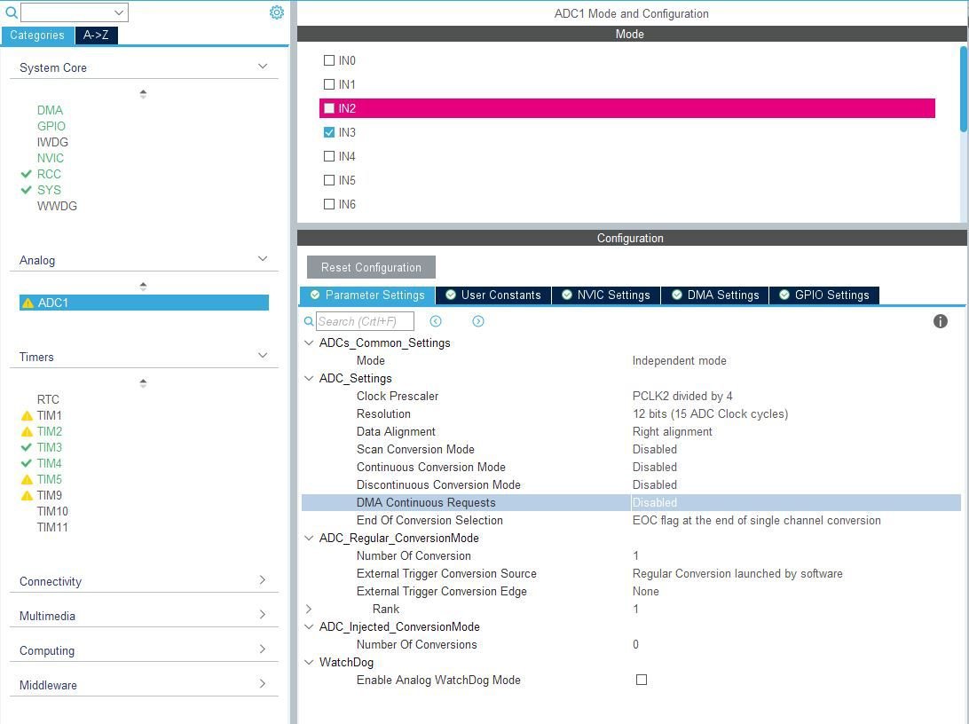
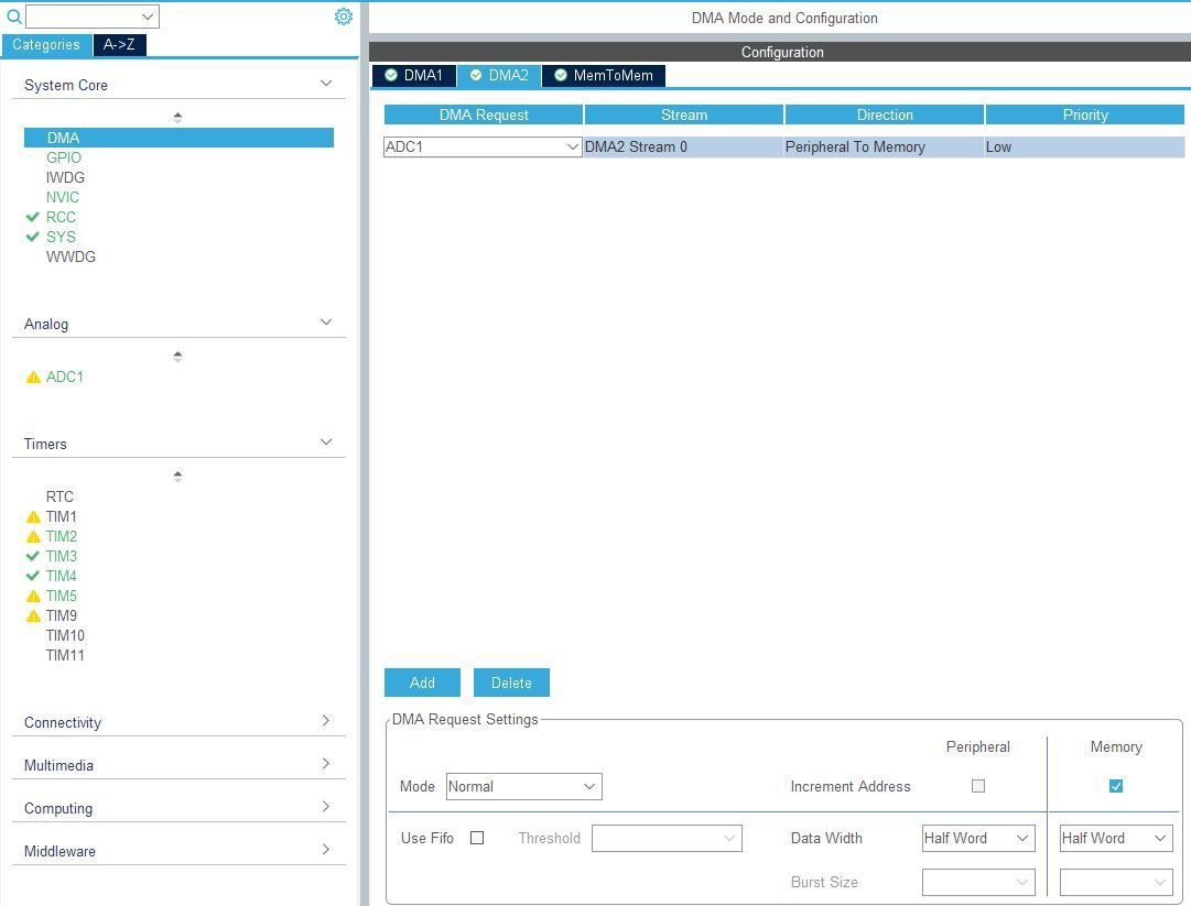
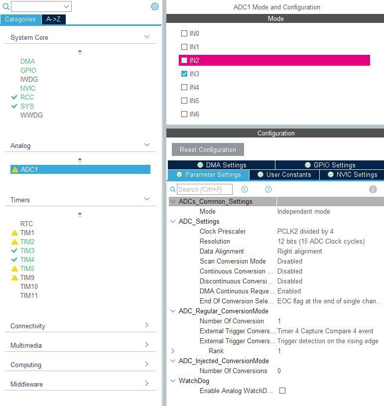
Let’s start with the ADC. We do not want to load the CPU with the handling of the ADC data so we use the MCU’s DMA (Direct Memory Access) which allows the ADC to write the memory without involving the CPU. So, first go to Analog, and select IN3 as the input of the ADC → this will make the PA3 pin as the input of the OS signal. Now as you enabled the ADC, go to System Core, select DMA, select the DMA2 tab and at the bottom click Add. A dropdown list will appear where you need to select ADC1. In the DMA Request Settings set the Mode to Normal. Then go back to the Analog/ADC1 settings. In the ADCSettings, enable only the DMA_ Continuous_Requests option. In the ADC_Regular_Conversion_Mode select the External Trigger Conversion Source as Timer 4 Capture Compare 4 event. Now, we are almost done with the ADC+DMA, but there is one thing that we need to check. When you press the save button the program automatically generates the code necessary to run all the peripherals and other things. However, sometimes the automatic code generation initializes the ADC1 before the DMA, which is wrong because in this case, the ADC will never start.
Make sure that above the /* USER CODE BEGIN 2 */ part in the main.c, the DMA is initialized first.
/* USER CODE BEGIN 0 */
#define CCDBuffer 6000
volatile uint16_t CCDPixelBuffer[CCDBuffer];
/* USER CODE END 0 */
Now we can read the ADC but we need to store the values somewhere and they need to be prepared for sending them to the PC via USB. Therefore we need a buffer that holds the data coming from the ADC. This is an array of 16-bit unsigned integers with the size of a large buffer. Let’s say we want to keep the things safe and allow some wiggle room, so we have a size of 6000.
/* USER CODE BEGIN 4 */
void HAL_ADC_ConvCpltCallback(ADC_HandleTypeDef* hadc)
{
CDC_Transmit_FS((uint8_t*) CCDPixelBuffer, CCDBuffer);
}
/* USER CODE END 4 */
We need to send the data to the computer via USB. Without any control, you can simply do that by calling the CDC_Transmit_FS() function inside the HAL_ADC_ConvCpltCallback(). Here, you have to pay a close attention to the data! The data from the MCU to the PC arrives in a binary format and the 12-bit number stored in a 16-bit unsigned integer is split into two, 8-bit integers. So, on your computer, on the receiving side, you need to reassemble the two 8-bit numbers into a 16-bit integer. Go to main.c, scroll down to the /* USER CODE BEGIN 4*/ part and use the following lines to send the buffer to the computer when a conversion is finished.
while (1)
{
/* USER CODE END WHILE */
/* USER CODE BEGIN 3 */
HAL_ADC_Start_DMA(&hadc1, (uint32_t*) CCDPixelBuffer, CCDBuffer);
}
/* USER CODE END 3 */
Finally, start the DMA in the while(1) loop.
If you did it right and followed my instructions precisely, you should see the data arriving to the computer. As a comparison, here is the image from the oscilloscope and from the software that I wrote to capture the CCD’s data coming from the MCU.

Output of the OS pin captured by an oscilloscope.

Output of the OS pin captured by the ADC and sent to the computer via USB. At this stage, this software is extremely rudimentary. Its only purpose is to show if we can successfully send the data to the computer, process it and display it.
The next steps will be to write a proper communication protocol for the MCU and improve the PC software. Also, I want to design a more compact PCB with smarter electronics, so I can utilize the whole range of the ADC.
The planned features of the software are the following:
Adjustment of integration time from the computer
Adjustment of the acquisition frequency (FPS) from the computer
Saving the data into a text file
Averaging multiple readings
…and many more
Hardware
Here you can see the most relevant hardware for the project. By clicking the pictures you will be redirected by my affiliate links so you can purchase the hardware and support me at the same time. Win-win!

STM32F401CCU6 microcontroller

TCD1304 Linear CCD

Test board (only PCB) for the TCD1304 Linear CCD based on the schematics found in the datasheet.